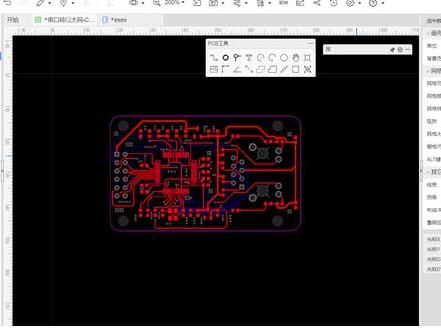
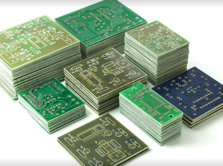
PCB design is pointer to circuit board design. Printed circuit board design is based on circuit schematic diagram, circuit designers need to achieve the function. The design of printed circuit board mainly refers to layout design, which needs to consider the layout of external connections, the optimal layout of internal electronic components, the optimal layout of metal connections and through holes, heat dissipation and other factors. Layout design needs the help of computer aided design (CAD). The layout design can save production cost and achieve good circuit performance and heat dissipation performance.

After the wiring design is completed, it is necessary to carefully check whether the wiring design conforms to the rules formulated by the designer, and also to confirm whether the rules formulated meet the requirements of the printed board production process. General check has the following aspects:
1, line and line, line and component pad, line and through hole, component pad and through hole, through hole and through hole between the distance is reasonable, whether to meet the production requirements.
2. Is the width of power line and ground line appropriate? Is there tight coupling between power supply and ground line (low wave impedance)? Is there a place in the PCB where the ground wire can be widened?
3. Whether measures are taken for key signal lines, such as short length, protective lines, input lines and output lines are clearly separated.
4, analog circuit and digital circuit part, whether there are independent ground wire.
5. Whether the graphics added to PCB will cause signal short circuit.

6. Modify some unsatisfactory lines.
7. Is there any process line on PCB? Whether the resistance welding meets the requirements of the production process, whether the resistance welding size is appropriate, whether the character mark is pressed on the welding pad of the device, so as not to affect the quality of electric equipment.
8. Whether the outer frame edge of the power supply layer in the multi-layer board is reduced, such as the copper foil exposed outside the board of the power supply layer is easy to cause short circuit.
In high speed design, the characteristic impedance of controllable impedance board and circuit is one of the important and common problems. Let's first understand the definition of transmission line: A transmission line consists of two conductors of a certain length, one for sending signals and the other for receiving signals (remember "loop" instead of "ground"). In a multilayer board, each line is part of a transmission line. The adjacent reference plane can be used as a second line or loop, and the key to a line becoming a "good performance" transmission line is to keep its characteristic impedance constant throughout the line.