

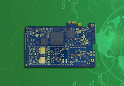


Model: high speed PCB
Layer: 8 Layer PCB
Material: Panasonic M6 high speed PCB
Finished Thickness: 1.0mm
Copper Thickness: 0.5OZ/1OZ
Color: Green/White
Surface treatment: Electric hard gold
Special technology: golden finger bevel
Min Trace / Space: 3mil/3mil
Application: Optical Module high speed PCB
What is high speed PCB?
High speed PCB uses such a circuit board, which is called high-speed circuit if the frequency of the digital logic circuit reaches or exceeds 45 MHZ~50 MHZ, and the circuit working on this frequency already accounts for one third of the entire electronic system.
How to choose PCB material for high speed design?
High speed PCB material requirements are as follows:
1. Low loss, CAF / heat resistance and mechanical toughness (adhesion) (good reliability)
2. Stable Dk / DF parameters (small variation coefficient with frequency and environment)
3. Small tolerance of material thickness and glue content (good impedance control)
4. Low copper foil surface roughness (reduce loss)
5. Try to choose glass fiber cloth with flat windows (reduce skew and loss)
The integrity of high-speed signal is mainly related to the consistency of impedance, transmission line loss and time delay. It can be considered that the signal integrity can be guaranteed if the appropriate waveform and eye diagram can be received at the receiving end. Therefore, the main parameter indexes of PCB material selection of high-speed digital circuit are DK, DF, loss, etc.
Whether analog circuit or digital circuit, the dielectric constant DK of high-speed PCB material is an important parameter for material selection, because DK value is closely related to the actual circuit impedance value applied to the material. When the DK value of high-speed PCB material changes, whether it changes with frequency or temperature, the transmission line impedance of the circuit will change unexpectedly, which will have an adverse impact on the signal transmission performance of high-speed digital circuit. If the DK of PCB material presents different values for harmonic components of different frequencies, the impedance will also have different resistance values at different frequencies. The unexpected change of DK value and impedance will lead to a certain degree of loss and frequency offset of harmonic components, distort the analog harmonic components of high-speed digital signals, and then reduce the integrity of the signal.
Dispersion closely related to DK value is also a characteristic of high-speed PCB materials. The smaller the change of DK value with frequency, the smaller the dispersion, and the better the application of high-speed digital circuits. The polarization of dielectric materials, the loss of high-speed PCB materials and the surface roughness of high-frequency copper conductors will cause the dispersion of the circuit. Therefore, the DK value of high-speed materials is required to be stable. Under different frequency bands and temperatures, the smaller the variation fluctuation, the better.
High speed PCB transmission line loss usually includes dielectric loss, conductor loss and radiation loss
Dielectric loss can also be called insulation loss. The insulation loss of high-speed PCB signal increases with the increase of frequency, especially with the change of frequency of high-order harmonic component of high-speed digital signal, it will produce serious amplitude attenuation, resulting in the distortion of high-speed digital signal. The dielectric loss is directly proportional to the signal frequency, the square root of the dielectric constant DK of the insulating layer and the dielectric loss factor DF of the insulating layer.
Conductor loss is related to the type of conductor (different types have different resistance), insulating layer and physical size of conductor, and is directly proportional to the square root of frequency; In the manufacturing of high-speed PCB, the main influence of using different substrates on conductor loss is caused by skin effect and surface roughness. When using different copper foil, the surface roughness of signal line is different. Affected by skin effect / depth, the length of copper tooth of copper foil will directly affect the transmission quality of high-speed signal. The shorter the length of copper tooth, the better the transmission quality of high-speed signal.
The radiation loss of high-speed PCB is related to dielectric characteristics and is directly proportional to the dielectric constant DK, dielectric loss factor DF and the square root of frequency.
Panasonic M6 high speed PCB material general properties
Item | Test method | Condition | Unit | MEGTRON6 | MEGTRON6 | |
Glass transition temp.(Tg) | DSC | A | °C | 185 | 185 | |
Thermal decomposition temp.(Td) | TGA | A | °C | 410 | 410 | |
CTE x-axis | α1 | IPC-TM-650 2.4.24 | A | ppm/°C | 14-16 | 14-16 |
CTE y-axis | 14-16 | 14-16 | ||||
CTE z-axis | α1 | IPC-TM-650 2.4.24 | A | 45 | 45 | |
α2 | 260 | 260 | ||||
T288(with copper) | IPC-TM-650 2.4.24.1 | A | min | >120 | >120 | |
Dielectric constant(Dk) | 12GHz | Balanced-type | C-24/23/50 | - | 3.4 | 3.6 |
Dissipation factor(Df) | 0.004 | 0.004 | ||||
Water absorption | IPC-TM-650 2.6.2.1 | D-24/23 | % | 0.14 | 0.14 | |
Flexural modulus | Fill | JIS C 6481 | A | GPa | 18 | 19 |
Peel strength* | 1oz(35μm) | IPC-TM-650 2.4.8 | A | kN/m | 0.8 | 0.8 |
What are the materials used for your high-speed PCB?
The usual answer is FR4. The PCB board we are talking about usually refers to the substrate. It is actually composed of copper foil and prepreg, and there are many classifications of copper foil and Prepreg according to different applications.
FR4 uses epoxy or modified epoxy resin as the adhesive, and glass fiber cloth as a kind of reinforcing material. That is to say, as long as the material of this system is used, it can be called FR4, so FR4 is the general term for this resin system. Printed boards using FR4 materials are currently the world's largest and most used type of printed boards.
Generally, FR4 will be classified according to the following types.
1. According to the naming and classification of fiberglass cloth weaving, such as:
106, 1067, 1080, 1078, 2116, 2113, 3313, 7628, etc.
These are commonly used glass cloth types, of course there are others. Each type of glass cloth is defined in the IPC specification. Therefore, the same type of glass cloth used by different PCB manufacturers is basically not much different, because glass cloth also has Many PCB manufacturers, but the same type of glass cloth provided by different PCB manufacturers must meet the requirements of the IPC specification.
2. Classified according to glass type
E-glass (E-glass): E stands for electrical, which means electrical insulating glass. It is a calcium aluminosilicate glass with little alkali metal oxide content (generally less than 1%), so it is also called alkali-free glass. Has high resistivity. E-glass has now become the most commonly used component of glass fiber, and many PCB material generally use E-glass unless otherwise specified.
NE glass (NE-glass): Also called low-Dk glass, it is a low-dielectric fiber glass developed by Japan Nitto Textile Co., Ltd., its dielectric constant ε (1MHz) is 4.6 (E glass is 6.6), and the loss factor The tanδ (1MHz) is 0.0007 (E glass is 0.0012), and NE-glass materials are commonly used such as M7NE, IT968SE and IT988GSE.
3. According to the resin system used by the PCB supplier and its performance classification:
Iteq high speed PCB material:
IT180A/IT170GRA1/IT958G/IT968/IT968SE/IT988GSE
Tuc high speed PCB material:
Tu862HF/Tu872LK/Tu872SLK/Tu872SLK-SP/Tu883/Tu933+
Panasonic high speed PCB material:
Megtron4/M4S/Megtron6/M6G/M7E/M7NE
Park Meteorwave series:
MW1000/2000/3000/4000/8000
ShengYi high speed PCB material: S1000-2(M)/S7439/S6, etc.
Rogers high speed PCB material: RO4003/RO3003/RO4350B (RF materials), etc.
4. Classification according to the loss level
It can be divided into ordinary loss sheet (Df≥0.02), medium loss sheet (0.01 5. Classification according to flame retardant performance Flame-retardant type (UL94-VO, UL94-V1) and non-flame-retardant type (UL94-HB grade) After reading the above introduction, returning to the previous question in our article, what high-speed PCB board do you usually use? Of course I want to hear the name of the material corresponding to the resin system and performance used by the PCB board supplier, such as IT180A/S1000-2/IT968/M4S, etc. According to different losses and materials from different manufacturers, it is mainly based on common medium and high-speed plates that have lower losses than ordinary FR4, while ordinary FR4, such as IT180A, S1000-2/M, Tu752/768, etc., basically have little difference in Df. It is also the Hi-Tg board we currently use most, Panasonic's Megtron6/M6G, which is used for high speed PCB. High speed PCB design, high speed PCB layout To design a high-quality high-speed PCB, we should consider signal integrity and power integrity. However, we know the difference between high-speed signal and high-frequency signal, and understand the difference between high-speed signal and high-frequency signal in PCB design. Although the direct result is from the signal integrity, we must not ignore the design of power integrity. Because the power integrity directly affects the signal integrity of the final high-speed PCB. When designing and building PCB stacks, priority must be given to material issues. 5g PCB must meet all specifications when carrying and receiving signal transmission, providing electrical connection and providing control for specific functions. In addition, PCB design challenges will need to be addressed, such as maintaining signal integrity at a high speed, heat dissipation management, and how to prevent electromagnetic interference (EMI) between data and boards Higher frequencies will require the use of appropriate materials in the PCB to capture and transmit both lower and higher signals without signal loss and EMI. Another problem is that the device will become lighter, more portable and smaller. Due to the strict weight, size and space constraints, PCB materials must be flexible and lightweight to accommodate all microelectronic devices on the circuit board. For PCB copper wiring, thinner wiring and stricter impedance control must be followed. The traditional subtraction etching process for 3G and 4G high-speed PCBs can be switched to a modified semi addition process. These improved semi addition processes will provide more accurate traces and straighter walls. Materials and substrates are also being redesigned. Printed circuit board companies are studying materials with dielectric constants as low as 3, because the standard materials for low-speed PCBs are usually 3.5 to 5.5. Tighter glass fiber braiding, lower loss factor, loss material and low profile copper will also be the choice of high-speed PCB for digital signals, so as to prevent signal loss and improve signal integrity. , crosstalk and parasitic capacitance are the main problems of circuit boards. In order to deal with crosstalk and EMI caused by analog and digital frequencies on the board, it is strongly recommended to route separately. The use of multilayer boards will provide better versatility to determine how to place high-speed routing, so as to keep the paths of analog and digital return signals away from each other, while keeping AC and DC circuits separate. Increasing shielding and filtering when arranging components should also reduce the amount of natural EMI on the PCB. In order to ensure that there are no defects and serious short circuits or open circuits on the copper surface, the advanced automatic optical inspection system (AIO) with higher functions and 2D metering will be used to check the routing of conductors and measure them. These technologies will help PCB manufacturers look for possible signal degradation risks. A higher signal speed will cause more heat to be generated by the current through the PCB. PCB materials for dielectric materials and core substrate layers will need to fully handle the high speed required by 5g technology. If the material is insufficient, it may lead to copper wiring, peeling, shrinkage and warpage, because these problems will lead to PCB deterioration. In order to cope with these higher temperatures, manufacturers will need to focus on material selection to solve the problems of thermal conductivity and thermal coefficient. Materials with higher thermal conductivity, excellent heat transfer and consistent dielectric constant must be used to produce good PCB. High-speed PCB design is a very complex design process. There are many factors to be considered in high-speed PCB design, which are sometimes opposite to each other. If the high-speed devices are arranged close to each other, although the delay can be reduced, crosstalk and significant thermal effect may occur. Therefore, in the design, it is necessary to weigh various factors and make a comprehensive compromise; It not only meets the design requirements, but also reduces the design complexity. The adoption of high-speed design PCB means constitutes the controllability of the design process. Only controllable can be reliable and successful high-speed PCB design! High-speed PCB, also known as high-speed PCB board or high-speed PCB board, is a high-speed PCB board manufactured with high-speed PCB material, with high speed, high reliability, low delay, large capacity, high bandwidth and other features. High-speed PCB is widely used in 5G communication such as 5G base stations and large computer. High-speed PCB circuit board is also one of the core products of IPCB. IPCB can provide users with high-speed PCB design, high-speed PCB samples, high-speed PCB manufacturing, SMT of high-speed PCB, and PCB assembly services. If you need high-frequency PCB manufacturing, please contact IPCB.
Model: high speed PCB
Layer: 8 Layer PCB
Material: Panasonic M6 high speed PCB
Finished Thickness: 1.0mm
Copper Thickness: 0.5OZ/1OZ
Color: Green/White
Surface treatment: Electric hard gold
Special technology: golden finger bevel
Min Trace / Space: 3mil/3mil
Application: Optical Module high speed PCB
For PCB technical problems, iPCB knowledgeable support team is here to help you with every step. You can also request PCB quotation here. Please contact E-mail sales@ipcb.com
We will respond very quickly.


