

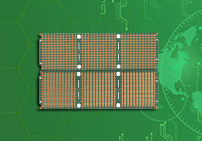


Model: Component Substrate PCB
Material: CC-HL820WDI
Layers: 2layers
Thickness: 0.3mm
Resistance welding: PSR-4000 WT03
Surface treatment: Hard Gold
Minimum aperture: 0.25mm
Minimum line distance: 75um
Minimum line width: 75um
Application: Electronic components Substrate
The substrate material used in Component Substrate PCB is the basic material for manufacturing semiconductor components and printed circuit boards, such as silicon, gallium arsenide, and silicon epitaxial garnet garnet used in the semiconductor industry. It is made of high-purity alumina (alumina) as the main raw material, which is formed by high-pressure molding, high-temperature firing, and then cut and polished. The ceramic substrate is the basic material for manufacturing thick film and thin film circuits. Copper clad laminate (referred to as clad laminate) is a substrate material used to manufacture printed circuit boards. In addition to supporting various components, it can also achieve electrical connection or electrical insulation between them.
The packaging substrate is an important part of electronic packaging and a bridge between the chip and the external circuit. The substrate plays the following roles in the package:
1. Realize the transmission of current and signal between the chip and the outside world;
2. Mechanically protect and support the chip;
3. It is the main way for the chip to dissipate heat to the outside world;
4. is the spatial transition between the chip and the external circuit.
From the material point of view, commonly used packaging substrates include metal substrates, ceramic substrates and organic substrates.
The metal substrate refers to a metal-based copper clad laminate made of a metal sheet, an insulating dielectric layer and a copper foil composite. Metal substrates are widely used in electronic components and integrated circuit support materials and heat sinks due to their excellent heat dissipation performance, mechanical processing performance, electromagnetic shielding performance, dimensional stability performance, magnetic performance and versatility. Power electronic devices (such as rectifier tubes, thyristors, power modules, laser diodes, microwave tubes, etc.) and microelectronic devices (such as computer CPUs, DSP chips) play an important role in the fields of microwave communication, automatic control, power conversion, and aerospace. Role.
Traditional metal-based electronic packaging materials include Invar, Kovar, W, Mo, Al, Cu, etc. These materials can partially meet the above-mentioned requirements, but still have many shortcomings. Invar is an iron-cobalt-nickel alloy, and Kovar is an iron-nickel alloy. They have good processing properties, low thermal expansion coefficient, but poor thermal conductivity; Mo and W have low thermal expansion coefficients, and thermal conductivity is much higher than Invar And Kovar, and the strength and hardness are very high, so Mo and W have been widely used in the power semiconductor industry.
However, Mo and W are expensive, difficult to process, poor in solderability, high in density, and have much lower thermal conductivity than pure Cu, which limits their further applications. Cu and Al have good thermal and electrical conductivity, but the coefficient of thermal expansion is too large, which is prone to thermal stress. The current metal substrate refers to a metal-based copper clad laminate made of a metal sheet, an insulating dielectric layer and a copper (or aluminum) foil composite.
The selection of substrate material for Component Substrate PCB must first consider the electrical characteristics of the substrate material, that is, the insulation resistance, arc resistance, and breakdown strength of the substrate; secondly, consider its mechanical characteristics, that is, the shear strength and hardness of the printed circuit board. ; In addition, price and PCB manufacturing costs must be considered.
Model: Component Substrate PCB
Material: CC-HL820WDI
Layers: 2layers
Thickness: 0.3mm
Resistance welding: PSR-4000 WT03
Surface treatment: Hard Gold
Minimum aperture: 0.25mm
Minimum line distance: 75um
Minimum line width: 75um
Application: Electronic components Substrate
For PCB technical problems, iPCB knowledgeable support team is here to help you with every step. You can also request PCB quotation here. Please contact E-mail sales@ipcb.com
We will respond very quickly.


