
Panasonic has developed a halogen-free ultra-low transmission loss PCB substrate (model: R-5515) suitable for millimeter wave antenna substrate, which achieves the highest low transmission loss in the industry with thermosetting resin.
With the development of ADAS (advanced driving support system) and autopilot, millimeter wave radar is used as the sensing technology to support these systems. For the antenna substrate for millimeter wave transceiver, low transmission loss is required. Now, as the substrate of antenna PCB, fluororesin substrate is mainly used. However, due to the characteristics of resin, it is difficult to process the substrate and the cost is high. This time, through Panasonic's Resin design technology and low coarsening copper foil bonding technology, "halogen free ultra-low transmission loss substrate material" with excellent low transmission loss and processability was realized.

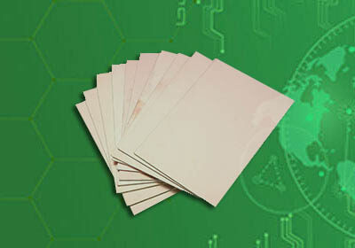
Characteristics of Panasonic R5515
Characteristics of Panasonic R5515
1. transmission loss: 0.079db/mm (@79ghz), low transmission loss, which can be used for high efficiency and low loss of millimeter wave antenna
From the point of view of processability and cost of antenna substrate, the market demand can replace the substrate material with high versatility which is the mainstream fluorine substrate. Through the exclusive resin design technology and low coarsening copper foil bonding technology, the company has developed a substrate material which can realize the lowest transmission loss in thermosetting resin. Through the same low transmission loss as fluororesin substrate, it contributes to the high efficiency and low loss of millimeter band antenna.
2. excellent PCB processability can reduce PCB processing cost
The PCB base material of PTFE is difficult to be drilled and copper plated in PCB. The loose r5515 is thermosetting resin material, and can be processed by PCB general equipment.
Due to the characteristics of the resin, it is difficult to drill holes and copper plating in the manufacture of fluororesin substrate. Because special manufacturing equipment is needed, the cost is too high. As this material is a thermosetting resin material, it can be easily processed by using the existing equipment for the general substrate. Therefore, the material can replace the fluororesin substrate material and contribute to reduce the processing cost of the substrate.
3. r5515 can be used to process mixed pressure PCB with general FR4
Because the Panasonic R5515 is a thermosetting resin material, it is easier to form at the same time as FR4.
With the development of miniaturization and low cost of millimeter wave band module, the multi-layer requirements of antenna integrated module substrate are higher and higher. Because the fluororesin substrate material is thermoplastic resin, it is difficult to form at the same time with glass epoxy substrate material of thermosetting resin, so it is difficult to realize multilayer. As this material is thermosetting resin material, it is easier to form at the same time with glass epoxy substrate material, which contributes to the multi-layer and cost reduction of antenna integrated module substrate.
Application of Panasonic r5515
Millimeter wave antenna PCB (PCB base material for antenna of vehicle millimeter wave radar and wireless communication base station), high speed PCB transmission.


