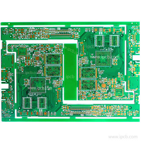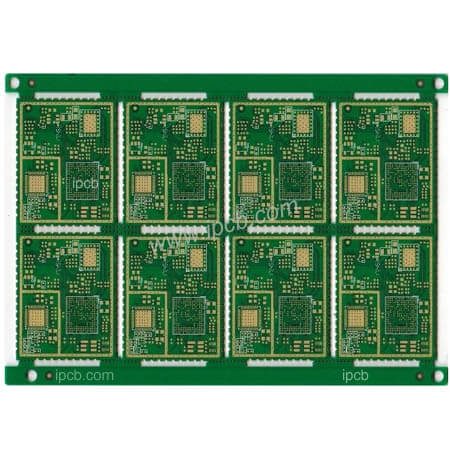
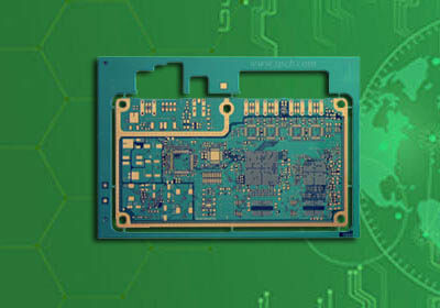

Model : Communication instrument Multilayer PCB
Material : Taiwan Tuc Tu-768
Layer : 10Layers
Color : Green/White
Finished Thickness : 1.6mm
Copper Thickness : 1OZ
Surface Treatment : Immersion Gold 2u"
Min Trace : 3mil(0.075mm)
Min Space : 3mil(0.075mm)
Characteristic : Need high precision impedance control
Application : Communication instrument PCB
TU-768 / TU-768P laminate / prepreg are made of high quality woven E-glass coated with the epoxy resin system, which provides the laminates with UV-block characteristic, and compatibility with automated optical inspection (AOI) process. These products are suitable for boards that need to survive severe thermal cycles, or to experience excessive assembly work. TU-768 laminates exhibit excellent CTE, superior chemical resistance and thermal stability plus CAF resistance property.

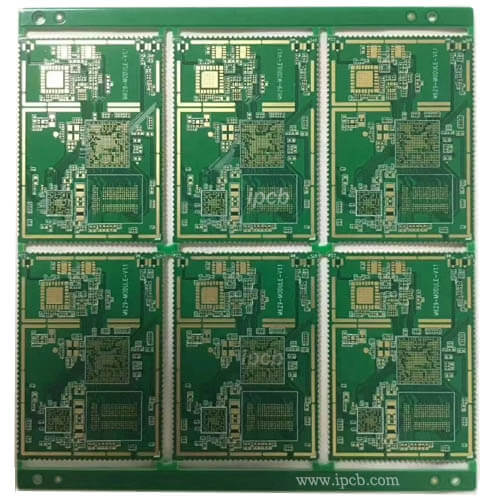
Tuc TU768 PCB
Communication equipment PCB requirements for materials
A very clear direction for communication equipment PCB is high-frequency and high-speed materials and board manufacturing. ipcb believes that in terms of high-frequency materials, it is obvious that leading material manufacturers in traditional high-speed fields such as Lianmao, Shengyi, Panasonic, and Taiyao have begun to deploy high-frequency plates and introduced a series of new materials. This will break the current dominance of Rogers in the field of high-frequency panels. After healthy competition, the performance, convenience and availability of materials will be greatly enhanced.
In terms of high-speed materials, ipcb believes that 400G products need to use M7N, MW4000 equivalent grade materials. In the backplane design, M7N is already the lowest loss option. In the future, backplanes/optical modules with larger capacity will require lower loss materials. The combination of resin, copper foil, and glass cloth will achieve the best balance between electrical performance and cost. In addition, the number of high-levels and high density will also bring reliability challenges.
Communication equipment PCB requirements for design
The selection of PCB board for communication equipment must meet the requirements of high frequency and high speed. The impedance matching, stacking planning, wiring spacing/holes, etc. must meet the signal integrity requirements, which can be specified from loss, embedding, high-frequency phase/amplitude, Start with six aspects of mixing, heat dissipation, and PIM.
Communication equipment PCB requirements for process technology
The improvement of the functions of communication equipment related applications will increase the demand for high-density PCBs, and HDI will also become an important technical field. Multi-level HDI products and even products with any level of interconnection will become popular, and new technologies such as buried resistance and buried capacitance will also have more and more applications.
In addition, PCB copper thickness uniformity, line width accuracy, interlayer alignment, interlayer dielectric thickness, control accuracy of back drilling depth, and plasma de-drilling ability are all worthy of in-depth study.
Communication equipment PCB requirements for equipment and instruments
High-precision equipment and pre-treatment lines with less roughening of the copper surface are currently ideal processing equipment; and the testing equipment includes passive intermodulation testers, flying probe impedance testers, loss test equipment, etc.
ipcb believes that sophisticated graphics transfer and vacuum etching equipment can monitor and feedback data changes in real-time line width and coupling distance detection equipment; electroplating equipment with good uniformity, high-precision lamination equipment, etc. can also meet the communication equipment PCB Production needs.
Communication equipment PCB requirements for quality monitoring
Due to the increase of the signal rate of communication equipment, the deviation of the board manufacturing has a greater impact on the signal performance, which requires stricter control of the production deviation of PCB manufacturing, and the existing mainstream board manufacturing process and equipment are not updated, which will become the future technology The bottleneck of development. How to break the situation for PCB manufacturers is of vital importance.
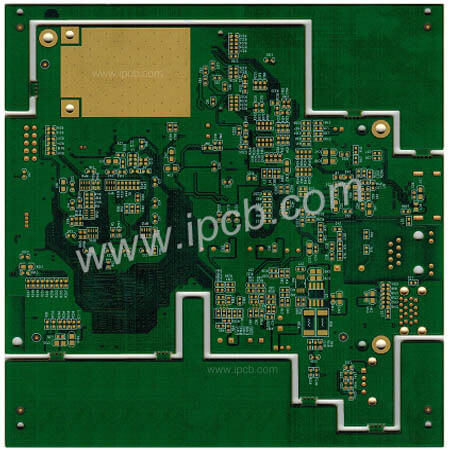
Model : Communication instrument Multilayer PCB
Material : Taiwan Tuc Tu-768
Layer : 10Layers
Color : Green/White
Finished Thickness : 1.6mm
Copper Thickness : 1OZ
Surface Treatment : Immersion Gold 2u"
Min Trace : 3mil(0.075mm)
Min Space : 3mil(0.075mm)
Characteristic : Need high precision impedance control
Application : Communication instrument PCB
For PCB technical problems, iPCB knowledgeable support team is here to help you with every step. You can also request PCB quotation here. Please contact E-mail sales@ipcb.com
We will respond very quickly.