
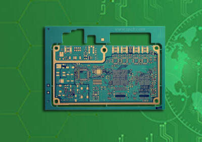


Model: Multilayer PCB
Material: KB6061, S1141, S1000, IT180
Layer: 4Layer - 48Layer Multilayer PCB
Solder Mask Color: Green/White/Blue/Red
Silk Screen Color: White/Black
Finished Thickness: 0.3mm - 6.0mm
Copper Thickness: 0.5-6OZ
Surface Treatment: Immersion Gold/OSP/HASL
Min Trace: 3mil(0.75mm)
Min Space: 3mil(0.75mm)
Application: Consumer electronics
Multilayer PCB is printed circuit board with more than 3 layer of circuit. Multilayer PCB design and multilayer PCB manufacturing are completed in even layer, so Multilayer PCB generally refers to 4 layer PCB, 6 layer PCB, 8 layer PCB... PCB Circuit board above.
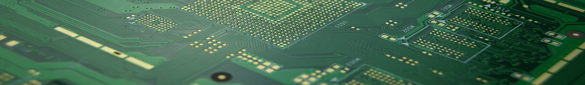
Multilayer PCB is PCB board made of multilayer copper foil conductive layer. The conductive copper foil appears to be the circuit layer of a polyhedral circuit board. Different layers are pressed together and then bonded together, and the insulating layer between layers is thermally protected. The multilayer PCB stack-up is placed in such a way that both sides of the PCB are on the surface. Through holes are used for electrical connection between different layers of Multilayer PCB circuit board. Due to the upgrading of the electronic industry, more and more multi-layer PCB is needed to meet the upgrading of electronic products.
With the continuous development of SMT technology and the continuous introduction of new generation SMD, such as QFP, QFN, CSP and BGA (especially MBGA), electronic products are more intelligent and miniaturized, which promotes the major reform and progress of PCB industrial technology. Since IBM first successfully developed high-density Multilayer PCB in 1991, multilayer PCB manufacturer have also developed a variety of high-density Multilayer PCB circuit board. The rapid development of multi-layer PCB manufacturing technology has promoted the multi layer PCB design to the direction of high-density wiring. Multilayer printed circuit board is widely used in the production of electronic products because of its flexible design, stable and reliable electrical performance and superior economic performance.
Since the middle and late 1980s, the output value of multilayer PCB printed circuit board has increased by more than 10% Due to the rapid development of components to "light, thin, short and small", multilayer board will become the most influential and vital category in the printed circuit board industry and become the leading product Multilayer printed circuit board structure will develop towards diversification, thin and high-rise Multi layer PCB requires high investment in equipment and technology. In the future, Multilayer PCB manufacturers will continue to introduce multilayer PCB manufacturing machines, high-level multilayer PCB will be produced by powerful multilayer PCB manufacturing.

multilayer PCB stack-up
Development trend of Multilayer PCB, 1-High density, 2-Thin multi-layer, ultra-high multi-layer board, 3-Diversification of Multilayer PCB structure, 4-Thin base material for high performance thin copper box, 5-PCB surface high flatness and surface coating technology, 6-multilayer flex PCB and rigid flexible multilayer PCB.
Difference between single layer and multilayer PCB
The biggest difference between PCB multi-layer board and single-sided PCB board and double-sided PCB board is the addition of internal power supply layer and grounding layer. The power supply and ground wire network are mainly wired on the power supply layer. However, multi-layer PCB wiring is mainly based on the top and bottom layers, supplemented by the middle wiring layer. Therefore, the design method of multi-layer PCB is basically the same as that of double-sided PCB. The key is how to optimize the wiring of internal electric layer to make the wiring of PCB circuit board more reasonable and better electromagnetic compatibility.
How to make multilayer PCB?
Fabrication process of multilayer PCB board, HASL PCB board / immersion gold PCB board
Ingredient - Inner - Layer - Bore hole - Sinking copper - Line - Graphic electricity - Etching - Resistance welding - Character - Tin spray (or gold deposit) - Gong edge - V cut (some plates do not need) - Flight test - Vacuum packaging
Fabrication process of gold plated PCB multilayer circuit board:
Cutting - Inner - Layer - Bore - Sink Copper - Line - Diagram - Electroplating - Gold - Etching - Resistance - Character - Gong Edge - V Section - Flight Test - Vacuum Packaging
The production of multi-layer PCB board requires not only high investment in technology and equipment, but also the accumulation of experience of technicians and producers. It is more difficult to process than traditional multilayer PCB board, and it requires high quality and reliability. So, what are the production process and key points of the multilayer PCB circuit board?
1. Selection of Multilayer PCB Material
With the high performance of electronic components. Multifunctional development with high frequencies. With the rapid development of signal transmission, low dielectric constant and dielectric loss of electronic circuit materials and low CTE are required. Low water absorption and better high performance copper clad plate materials to meet the processing and reliability requirements of multilayer PCB plates.
2. Design of laminated multilayer PCB structure
The main factor to be considered in the design of PCB laminated structures is the heat resistance of the materials. Voltage resistance. The following principles should be followed in terms of filling capacity and dielectric layer thickness:
(1) The semi-cured sheet must be consistent with the core plate manufacturer.
(2) When customers require high TG plates, the core plate and semi-cured sheet should use the corresponding high TG materials.
(3) Semi-cured sheets with high resin content are selected for the inner baseboard 3OZ or above.
(4) If there is no special requirement from the customer, the dielectric layer thickness tolerance is generally controlled by +/-10%, and for impedance plates, the dielectric thickness tolerance is controlled by IPC-4101C/M tolerance.
3. Inter-Layer Alignment Control for Multilayer PCB
Precision and production dimension control of inner core plate size compensation requires precise compensation of graphical dimensions of each layer of multilayer PCB board through the data collected in production and historical data experience in a certain time to ensure consistency of core plate expansion and contraction.
4. Inner circuit technology of multilayer PCB
For the production of multilayer PCB boards, laser direct imager (LDI) can be introduced to improve the graphics resolution ability. In order to improve the line etching ability, the line width and the pad need to be compensated appropriately in engineering design to confirm the inner line width. Line spacing. Isolation ring size. Independent lines. Is the design compensation for hole-to-line distance reasonable, otherwise change the design of the project.
5. Compression process for multilayer PCB
Currently, the inter-layer positioning methods mainly include: four-slot positioning (PinLAM). Hot melt. Rivet. Combining hot melting with rivet, different product structures have different positioning modes.
6. Boring Technology for Multilayer PCB
Due to the overlap of layers, the sheet and copper layers are very thick, which causes serious wear and tear on the drill head and easily breaks the drill, for the number of holes. Down and rotate properly.

Multilayer PCB manufacturing process
Ordinary PCB circuit boards are divided into single-sided routing and double-sided routing. They are single-sided PCB boards and double-sided PCB boards. However, due to product space design factors, electronic products can be superimposed with multiple layers in addition to surface wiring. In the production process, after each layer of circuit is made, it is positioned and pressed by optical equipment, so that the multilayer circuit is superimposed on a PCB circuit board. Commonly known as multilayer PCB. Any circuit board with more than or equal to 3 layers can be called a multilayer circuit board. Multilayer circuit boards can be divided into multilayer rigid circuit boards, multilayer soft and hard circuit boards, and multilayer soft and hard circuit boards. The multi-layer PCB circuit board is the size of the PCB area and the difficulty of the manufacturing process to calculate multilayer PCB manufacturing price.
IPCB is a multilayer PCB manufacturer. We provide high-volume multilayer PCB manufacturing, cheap multilayer PCB and high quality multilayer PCB. We provide you with high-quality multi-layer PCB prototyping services. Provide you with satisfactory multilayer PCB prototyping service.
Model: Multilayer PCB
Material: KB6061, S1141, S1000, IT180
Layer: 4Layer - 48Layer Multilayer PCB
Solder Mask Color: Green/White/Blue/Red
Silk Screen Color: White/Black
Finished Thickness: 0.3mm - 6.0mm
Copper Thickness: 0.5-6OZ
Surface Treatment: Immersion Gold/OSP/HASL
Min Trace: 3mil(0.75mm)
Min Space: 3mil(0.75mm)
Application: Consumer electronics
For PCB technical problems, iPCB knowledgeable support team is here to help you with every step. You can also request PCB quotation here. Please contact E-mail sales@ipcb.com
We will respond very quickly.


