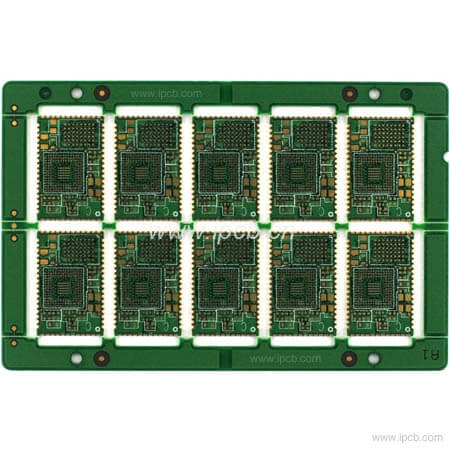
commonly used PCB board detection methods
The purpose of detecting PCB boards is to find out the defects of PCB boards and repair them, to ensure the production quality of the circuit boards, and to improve the product qualification rate. At present, PCB inspection methods can be divided into two categories: electrical testing methods and visual testing methods. Today I will share with you 7 commonly used PCB detection methods, as follows:
1. Manual visual inspection test
Manual visual inspection of PCB is the most traditional inspection method, the advantage is that the initial cost is low and there is no test fixture. By visual inspection with a magnifying glass or a calibrated microscope, judge whether the PCB board is qualified, and determine when the correction operation is needed. The disadvantages of manual visual inspection are subjective human error, high long-term cost, discontinuous defect detection and difficulty in data collection. With the increase in PCB production and the shrinking of the wire spacing and component volume on the PCB, manual visual inspection methods are becoming more and more infeasible.

2. Size check
Use a two-dimensional image measuring instrument to measure the position, length and width of the hole, position and other dimensions. Since the PCB is a thin and soft product, it is easy to deform in contact measurement, resulting in inaccurate measurement. The two-dimensional image measuring instrument has become the best high-precision dimension measuring instrument. The image measuring instrument can realize automatic measurement after programming, which not only has high measurement accuracy, but also greatly shortens the measurement time and improves the measurement efficiency.
3. Online test
There are several test methods, such as bed of needle tester and flying probe tester. Identify manufacturing defects through electrical performance testing, and test analog-digital and mixed-signal components to ensure they meet specifications. The main advantages are the low test cost of each board, powerful digital and functional test functions, fast and thorough short-circuit and open-circuit tests, programming firmware, high defect coverage, and easy programming. The main disadvantages are the need to test fixtures, programming and debugging time, fixture manufacturing costs and difficult to use.
4. Functional system test
Functional testing is the earliest automatic testing principle. It is a comprehensive test of circuit board functional modules using special test equipment in the middle and end of the production line to confirm the quality of the circuit board. Functional system testing is based on a specific board or a specific unit, and can be done using various devices. There are final product testing, the latest physical model and stack testing. Functional testing usually does not provide in-depth data to improve the process, but requires special equipment and specially designed test procedures. Because it is very complicated to write functional test programs, it is not suitable for most circuit board production lines.
5. Laser detection system
Laser inspection is to scan the printed board with a laser beam, collect all measurement data, and compare the actual measurement value with the preset qualified limit value. This is the latest development of PCB testing technology, which has been verified on bare boards and is being considered for assembly board testing. The main advantage is fast output, no fixtures and barrier-free visual access; the disadvantage is high initial cost, maintenance and use problems.
6. Automatic X-ray inspection
Automatic X-ray inspection is mainly used to detect defects in ultra-fine pitch and ultra-high-density circuit boards, as well as bridges, missing chips, poor alignment and other defects generated during the assembly process. The inspection principle is to use the difference in X-ray absorption rate of different substances to inspect the parts to be tested and find defects. Tomography can also be used to detect internal defects in IC chips, which is the only way to test the soldering quality of ball grid arrays and solder balls. The main advantage is the ability to check the quality of BGA soldering and embedded components without the need to spend fixtures.
7. Automatic optical inspection
Automatic optical inspection, also known as automatic visual inspection, is a relatively new method of identifying manufacturing defects. It is based on optical principles, and comprehensively uses image analysis, computer and automatic control technology to detect and deal with defects encountered in production. AOI is usually used before and after reflow and before electrical testing to improve the pass rate of electrical processing or functional testing. At this time, the cost of correcting the defect is much lower than the cost after the final test, generally more than ten times.
The above are the 7 commonly used PCB inspection methods. Although there are many PCB inspection methods, the most popular ones on the market are optical inspection and X-ray inspection.