There are single-sided, double-sided and multi-layer PCB boards. There is no restriction on the number of multilayer boards. There are currently more than 100-layer PCBs. Common multi-layer PCBs include four-layer boards and six-layer boards. So why do people have such questions as "Why multilayer circuit boards are even-numbered layers"? Relatively speaking, even-numbered PCBs do have more than odd-numbered PCBs, and they have more advantages.
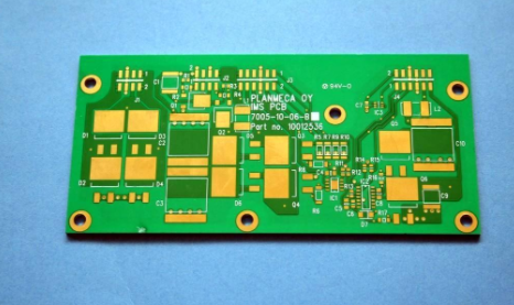
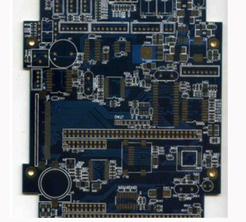
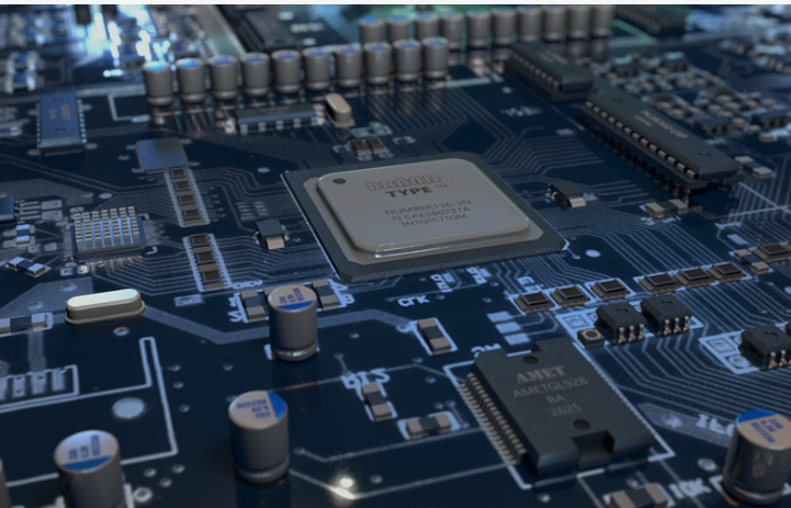
Multilayer circuit board
Because of the short layer of dielectric and foil, the raw material cost of odd-numbered PCBs is slightly lower than that of even-numbered PCBs. However, the processing cost of odd-numbered PCBs is significantly higher than that of even-numbered PCBs. The processing cost of the inner layer is the same, but the foil/core structure obviously adds to the processing cost of the outer layer.
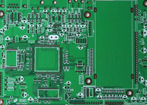
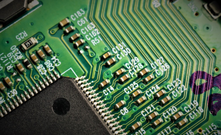
Odd-numbered PCBs require a non-standard laminated core layer bonding process to be added to the core structure process. Compared with the nuclear structure, the production power of the factory that adds foil to the nuclear structure will be reduced. Prior to lamination and bonding, the outer core requires a specified treatment, which adds the risk of scratches and etching errors on the outer layer. Printed circuit board
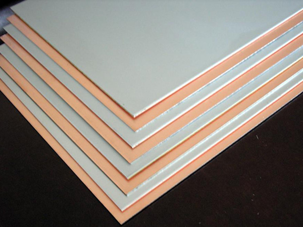
Balance structure to avoid twists and turns

The reason why odd-numbered layers are not used in multi-layer circuit boards is that odd-numbered circuit boards are simply twists and turns. When the PCB is cooled after the multilayer circuit bonding process, the different lamination tensions of the core structure and the foil-clad structure will cause the PCB to bend. With the increase in the thickness of the circuit board, the risk of bending of the two different structures of the composite PCB also increases. The key to eliminating circuit board twists is to use balanced stacking. Although a PCB with a certain degree of tortuosity meets the requirements of the specification, the subsequent processing power will be reduced, resulting in an increase in cost. Because special equipment and craftsmanship are required during assembly, the precision of component placement is reduced, and then the quality is impaired.
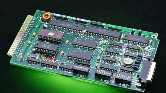
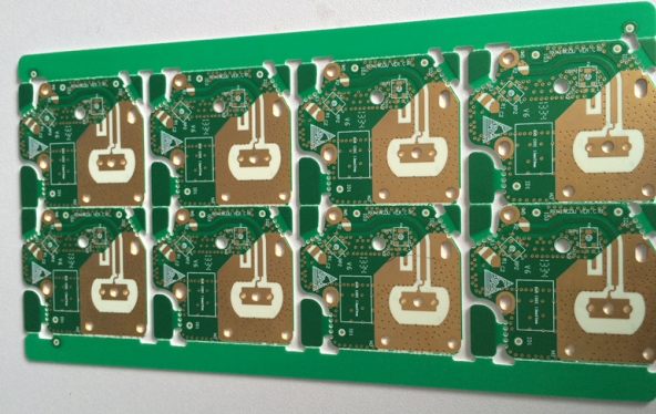
To put it simply, in the PCB process, a four-layer board is better than a three-layer board, mainly in terms of symmetry. The warpage of the four-layer board can be controlled below 0.7% (IPC600 specification), but when the size of the three-layer board is large, the warpage will exceed this specification, affecting the reliability of the SMT patch and the entire product. Therefore, ordinary planners will not plan odd-numbered floors. Even if the odd-numbered floors have achieved their functions, they will be planned as fake even-numbered floors, that is, the 5 floors are planned into 6 floors, and the 7 floors are planned into 8 floors. Double layer circuit board
Because of the above reasons, most multi-layer circuit boards are planned as even-numbered layers, with few odd-numbered layers.
Shenzhen Wanchuangxing Electronics Co., Ltd. was established in 2011. It is a professional manufacturer of allegro and model enterprises in small and medium batches. The company is located in Lisheng Industrial Park, Tangwei, Fuyong, Bao'an District, Shenzhen. It has a 16,000 square meter factory building. The monthly production capacity of the batch line reaches 10,000 square meters, and the monthly production variety of the model line reaches 3,000.