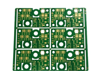
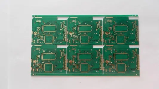
Printed circuit board(PCB-Printed Circuit Board) is also called printed circuit board, printed circuit board. Multi-layer PCB printed board refers to a printed board with more than two layers. It is composed of connecting wires on several layers of insulating substrates and pads for assembling and welding electronic components. The role of insulation. With the continuous development of SMT (Surface Mount Technology) and the continuous introduction of a new generation of SMD (Surface Mount Devices), such as QFP, QFN, CSP, BGA (especially MBGA), electronic products are becoming more intelligent and miniaturized. Promoted major reforms and advances in PCB industrial technology. Since IBM first successfully developed high-density multilayer (SLC) in 1991, major groups in various countries have also developed various high-density interconnect (HDI) microplates. The rapid development of these processing technologies has prompted the design of PCBs to gradually develop in the direction of multi-layer, high-density wiring. With its flexible design, stable and reliable electrical performance and superior economic performance, multilayer printed boards have been widely used in the production of electronic products.

Next, with years of experience in designing printed boards, the author focuses on the electrical performance of printed boards, combined with process requirements, and discusses the basic essentials of multi-layer board design from the aspects of stability and reliability of printed boards.
two. Necessary work before printed board design
Check the schematic diagram carefully: the design of any printed board is inseparable from the schematic diagram. The accuracy of the schematic diagram is the prerequisite basis for the correctness of the printed board. Therefore, before the design of the printed board, the signal integrity of the schematic must be carefully and repeatedly checked to ensure the correct connection between the devices.
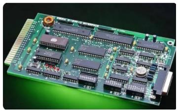
Device selection: The selection of components is a very important link for the design of printed boards. Devices with the same functions and parameters may have different packaging methods. The package is different, and the solder holes (disks) of the components on the printed board are different. Therefore, before embarking on the printed board design, we must determine the packaging form of each component.
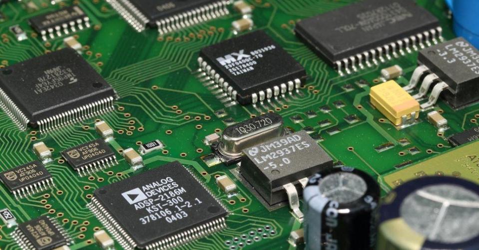
Multilayer boardsmust be positioned in the selection of surface mount components (SMD) in terms of device selection. SMD is widely used in various electronic products due to its advantages of miniaturization, high integration, high reliability, and installation automation. . At the same time, in the selection of devices, not only should the characteristic parameters of the device meet the needs of the circuit, but also the supply of the device to avoid the problem of device shutdown. At the same time, it should be aware that many domestic devices such as chip resistors, capacitors, and connections The quality of potentiometers and potentiometers has gradually reached the level of imported components, and has the advantages of sufficient supply, short delivery time, and low price. Therefore, under the condition of circuit permission, domestic devices should be considered as far as possible.