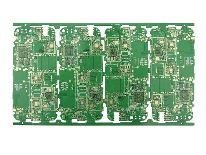
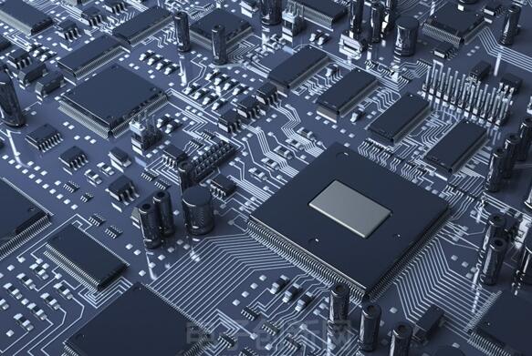
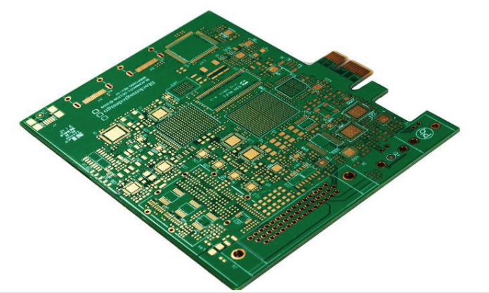
Three requirements for a good PCB circuit board
To make circuit boards, everyone and every circuit board manufacturer wants to be better, so what should we do if we want to make circuit boards better? Next, let’s talk about 3 points we need to do:
Set clear goals
When doing a task, we must clarify his design goal, whether it is an ordinary PCB board, a high frequency PCB board, a small signal processing PCB board or a PCB board with both high frequency and small signal processing. If it is an ordinary PCB board, The layout and wiring should be reasonable and tidy, and the mechanical dimensions should be accurate. If there are medium load lines and long lines, certain methods must be used to deal with them to reduce the load. Special consideration should be given to these signal lines when the signal lines are used.
According to the network theory of distributed parameters, the interaction between high-speed circuits and their connections is a decisive factor that cannot be ignored in system design. As the transmission speed of the gate increases, the opposition on the signal line will increase the crosstalk between adjacent signal lines. Proportionally increasing the power consumption and heat dissipation of the usual high-speed circuits are also great.

Enough attention should be paid to high-speed PCBs. When there are millivolt or even microvolt-level weak signals on the board, special care is needed for these signal lines. Small signals are too weak and are very susceptible to interference from other strong signals. Shielding measures are often It is necessary, otherwise it will greatly reduce the signal-to-noise ratio so that the useful signal is submerged by noise and cannot be effectively extracted. The commissioning of the board should also be considered in the design stage. The physical location of the test point. The isolation of the test point and other factors cannot be ignored because it is somewhat small. Signals and high-frequency signals cannot be directly added to the probe for measurement. In addition, other related factors such as the number of layers of the board and the mechanical strength of the package shape of the component should be considered before making the PCB board. The design goals are well known.
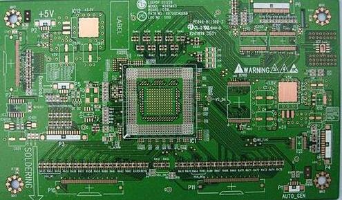
Consider the layout of components
The first factor to consider is the electrical performance. Put the closely related components together as much as possible. Especially for some high-speed line layouts, it is necessary to make it as short as possible. Power signals and small signal components should be separated to meet the premise of circuit performance. Next, the components should be placed neatly and beautifully to facilitate the testing of the mechanical size of the board. The location of the sockets should also be carefully considered. The grounding and the transmission delay time of the interconnection line in the high-speed system are also the first factors to be considered in the system design. Signal line The transmission time of the above has a great influence on the overall system speed, especially for the high-speed ECL circuit. Although the integrated circuit block itself has a high speed, because the ordinary interconnection line on the bottom board has a delay of about 2ns per 30cm line length The increase in delay time can greatly reduce the system speed. Like a shift register synchronous counter.
This kind of synchronous working parts is best placed on the same plug-in board because the transmission delay time of the clock signal to different plug-in boards is not equal, which may cause the shift register to produce a major error. If it cannot be placed on one board, synchronization is critical. The length of the clock line from the common clock source to each plug-in board must be equal. The consideration of four pairs of wiring. With the completion of the design of OTNI and star optical fiber network, there will be more basic concepts with high-speed signal lines above 100MHz.
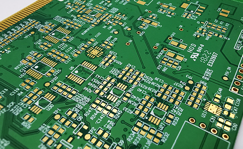
Know the requirements of the layout and routing of the functions of the components we use
We know that some special components have special requirements in the layout and wiring. For example, the analog signal amplifier used by LOTI and APH. The analog signal amplifier requires a smooth ripple for the power supply. The small analog small signal part should be as far away from the power device as possible. Some parts are also specially equipped with a shielding cover to shield the stray electromagnetic interference. The GLINK chip used on the NTOI board uses the ECL process. The power consumption is large and the heat is severe. For the heat dissipation problem, special consideration must be made in the layout. If natural heat dissipation is used.
Place the GLINK chip in a place where the air circulation is relatively smooth and the heat emitted cannot have a big impact on other chips. If the board is equipped with speakers or other high-power devices, it may cause serious pollution to the power supply. This should also be caused. Enough attention...
Summarize
I believe that as long as we pay attention to 3 points, it is very possible to produce good PCB boards, and the circuit board manufacturers who do not stick to these points, so the quality of the PCB boards they produce is very reliable.