Designing and building next-generation electronic products is a complex process, especially in a highly competitive global industry such as the electronics industry, where rapid and continuous technological change has become a common thing and a rule of innovation. If the designer cannot accept these changes, he will face the risk of being left behind by his competitors, or even be unable to join the competition at all. This situation is particularly obvious for PCB design. In this market, consumers prefer electronic products with smaller size, lower price, faster speed and more functions. Coupled with the ever-shortening design cycle and geographically dispersed design teams, they are constantly advancing the design. Complexity, and push the use of traditional design tools to its limit. The increase in the number of networks, stricter design constraints and wiring density, and the gradual migration to high-speed and high-density projects have further aggravated the complexity of PCBs. This trend is affecting all areas of the industry, not just high-end consumer electronics.

Fortunately, PCB design tools have been steadily developed in recent years to meet the challenges posed by this increasingly complex design field. A major change-the adoption of 3D functions, is expected to allow designers to take into account design innovation and competitiveness in the global market.
Challenges of design in the 3D world
Traditionally, circuit board designers have relied on design prototypes to ensure the shape, fit, and functionality of the design before PCB manufacturing. Although feasible, this method has many disadvantages. First, the designer cannot be sure whether the circuit board is suitable until the actual prototype is manufactured. Secondly, this method generally leads to multiple prototypes during the design process. Furthermore, multiple prototypes are very time-consuming, and the average cost for a moderately complex design prototype is US$8,929. Any additional time or cost increase in the design process will not only affect the competitiveness of a company, but also hinder us from entering new businesses. It is not difficult to understand why this method is unpopular.
Another drawback is that PCB design is traditionally a two-dimensional design. Basically, the design is created in 2D, after manual annotation, it is passed to the mechanical design engineer. Mechanical engineers use mechanical CAD software to redraw the design in 3D. Because it is completely manual, this method is very time-consuming and error-prone. Therefore, it cannot provide competitive differentiation for designing next-generation electronic products. Now that the problem is obvious, circuit board designers need to find better ways to view and analyze their increasingly complex designs.
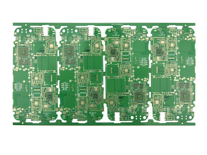
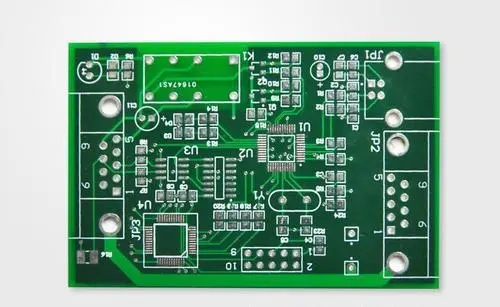
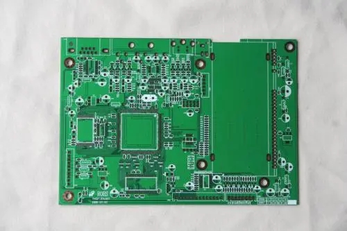
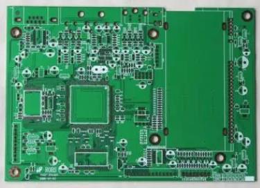
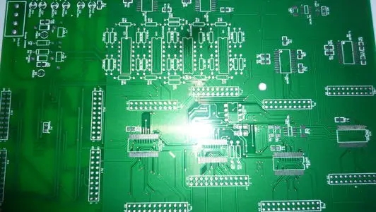
The ultimate goal of PCB designers is to create products for the real world (with 3 dimensions), so the best solution is to use a design tool with advanced 3D functions. It allows designers to view the real 3D image of the design before production, eliminating the need to make prototypes, saving time and money (Figure 1). You can easily generate accurate 3D models, and then use them for circuit board layout in real 3D. In addition, the 3D model of the target shell can also be imported into the PCB design to ensure that the designed circuit board can be perfectly placed in this shell. Later, the designers were able to confidently submit their design documents for production.