The choice of surface treatment process The choice of surface treatment process mainly depends on the type of final assembled components; the surface treatment process will affect the production, assembly and final use of PCB. The following will specifically introduce the use occasions of five common surface treatment processes.
1. Hot air leveling Hot air leveling used to dominate the PCB surface treatment process. In the 1980s, more than three-quarters of PCBs used hot air leveling processes, but the industry has been reducing the use of hot air leveling processes in the past ten years. It is estimated that about 25%-40% of PCBs currently use hot air. Leveling process. The hot air leveling process is dirty, unpleasant, and dangerous, so it has never been a favorite process, but hot air leveling is an excellent process for larger components and wires with larger spacing.
In high-density PCBs, the flatness of hot air leveling will affect subsequent assembly; therefore, HDI boards generally do not use hot air leveling processes. With the advancement of technology, the industry now has a hot air leveling process suitable for assembling QFPs and BGAs with smaller pitches, but there are fewer practical applications. At present, some factories use organic coating and electroless nickel/immersion gold processes instead of hot air leveling processes; technological developments have also led some factories to adopt tin and silver immersion processes. Coupled with the lead-free trend in recent years, the use of hot air leveling has been further restricted. Although the so-called lead-free hot air leveling has appeared, this may involve equipment compatibility issues.
2. Organic coating It is estimated that about 25%-30% of PCBs currently use organic coating technology, and the proportion has been rising (it is likely that organic coating has now surpassed hot air leveling in the first place). The organic coating process can be used on low-tech PCBs or high-tech PCBs, such as PCBs for single-sided TVs and boards for high-density chip packaging. For BGA, there are also more applications of organic coating. If PCB does not have functional requirements for surface connection or a limitation of storage period, organic coating will be the most ideal surface treatment process.

3. The process of electroless nickel/immersion gold electroless nickel/immersion gold is different from organic coating. It is mainly used on boards that have functional requirements for connection and a longer storage period, such as mobile phone keypads and router housings. An electrical contact area where the edge connection area and the chip processor are elastically connected. Due to the flatness problem of hot air leveling and the removal of organic coating flux, electroless nickel/immersion gold was widely used in the 1990s; later, due to the appearance of black disks and brittle nickel-phosphorus alloys, electroless nickel plating /The application of immersion gold process has decreased, but at present almost every high-tech PCB factory has electroless nickel plating/immersion gold wire.
Considering that the solder joint will become brittle when removing the copper-tin intermetallic compound, there will be many problems in the relatively brittle nickel-tin intermetallic compound. Therefore, portable electronic products (such as mobile phones) almost all use organic coating, immersion silver or immersion tin formed copper-tin intermetallic compound solder joints, while electroless nickel/immersion gold is used to form the button area, contact area and EMI shielding area . It is estimated that about 10%-20% of PCBs currently use electroless nickel/immersion gold processes.
4. Immersion silver for circuit board proofing is cheaper than electroless nickel/immersion gold. If the PCB has connection functional requirements and needs to reduce costs, immersion silver is a good choice; coupled with the good flatness and contact of immersion silver, Then we should choose the immersion silver process. There are many immersion silver applications in communication products, automobiles, and computer peripherals, and immersion silver also has applications in high-speed signal design.
Because immersion silver has good electrical properties that other surface treatments cannot match, it can also be used in high-frequency signals. EMS recommends the immersion silver process because it is easy to assemble and has better checkability. However, due to defects such as tarnishing and solder joint voids, the growth of immersion silver has been slow (but not decreased). It is estimated that about 10%-15% of PCBs currently use the immersion silver process.
5. Immersion tin tin was introduced into the surface treatment process in the past ten years, and the emergence of this process is the result of the requirements of production automation. Immersion tin does not bring any new elements into the solder joints, which is especially suitable for backplanes for communications. Tin will lose its solderability beyond the storage period of the board, so immersion tin requires better storage conditions. In addition, the immersion tin process has been restricted in its use due to the carcinogenic substances contained in it.
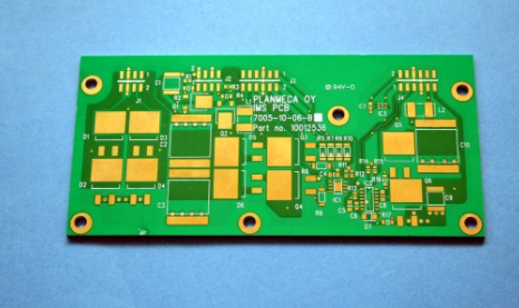
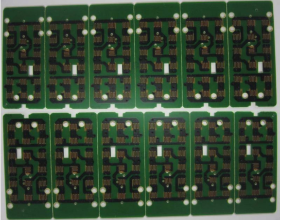
It is estimated that about 5%-10% of PCBs currently use the immersion tin process. PCB proofing
With the increasing requirements of customers, stricter environmental requirements, and more and more surface treatment processes, the choice of surface treatment processes that have development prospects and more versatility seems to be a bit dazzling and confusing at present. . Where the PCB surface treatment process will go in the future, it is impossible to predict accurately now