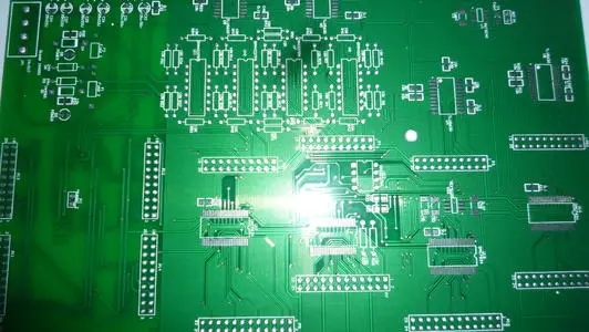
1. PCB current and line width
The current carrying capacity of the PCB board depends on the following factors: line width, line thickness (copper foil thickness), and allowable temperature rise. Everyone knows that the wider the PCB trace, the greater the current-carrying capacity. Assuming that under the same conditions, a 10MIL trace can withstand 1A, how much current can a 50MIL trace withstand, is it 5A? The answer is naturally no. Please look at the following data from international authorities:
Data provided:
The unit of line width is: Inch (1inch=2.54cm=25.4mm)
Data source: MIL-STD-275 Printed Wiring for Electronic Equipment

2. PCB design copper platinum thickness, line width and current relationship
Before understanding the relationship between PCB design copper platinum thickness, line width and current, let us first understand the conversion between ounces, inches and millimeters of PCB copper thickness: "In many data sheets, PCB copper thickness is often used in ounces. As a unit, its conversion relationship with inches and millimeters is as follows:
1 ounce = 0.0014 inches = 0.0356 millimeters (mm)
2 ounces = 0.0028 inches = 0.0712 millimeters (mm)
Ounce is a unit of weight, and the reason why it can be converted to millimeters is because the thickness of the copper coating of the PCB board is ounces/square inch"
You can also use the empirical formula to calculate: 0.15 * line width (W) = A
The above data are all line current carrying values at a temperature of 25°C.
Wire impedance: 0.0005*L/W (line length/line width)
The current carrying value is directly related to the number of components/pads and vias on the line
In addition, the relationship between the current carrying value of the wire and the number of vias pads of the wire
1. The load-bearing value listed in the table data is the maximum current load-bearing value at a normal temperature of 25 degrees. Therefore, various environments, manufacturing processes, plate processes, plate quality, etc. must be considered in the actual design. Kinds of factors. Therefore, the table is provided only as a reference value.
2. In the actual design, each wire will also be affected by the pads and vias, such as the line segment with a lot of pads, after tinning, the current carrying value of the pad section will greatly increase, maybe Many people have seen that a certain section of the line between the pad and the pad in some high-current boards is burned. The reason is very simple. The pad has component feet and solder after the tin is completed, and the current of that section of the wire is increased. The maximum current carrying value of the pad between the pad and the pad is the maximum current carrying value allowed by the wire width. Therefore, when the circuit fluctuates momentarily, it is easy to burn the section of the line between the pad and the pad. The solution: increase the width of the wire. You can add a wire of about 0.6 Solder layer to the wire, of course, you also add a 1mm Solder layer wire) So after tinning, this 1mm wire can be regarded as a 1.5mm~2mm wire (depending on the wire) The uniformity and amount of tin when tin is passed)
3. The processing method around the pad in the figure is also to increase the uniformity of the current carrying capacity of the wire and the pad. This is especially true in the board with large current and thick pins (the pin is greater than 1.2, and the pad is above 3). Very important. Because if the pad is above 3mm and the pin is above 1.2, the current of the pad will increase dozens of times after tinning. If there is a large fluctuation in the moment of large current, the current of the entire line The carrying capacity will be very uneven (especially when there are many pads), and it is still easy to cause the possibility of the circuit between the pads and the pads to burn. The processing in the figure can effectively disperse the uniformity of the current carrying value of a single pad and surrounding lines.
Finally, explain again: the current carrying value data table is only an absolute reference value. When not doing large current design, an additional 10% of the data provided in the table can definitely meet the design requirements. In the general single-panel design, the copper thickness is 35um, which can basically be designed at a ratio of 1:1, that is, 1A current can be designed with a 1mm wire, which can meet the requirements (calculated at a temperature of 105 degrees) .
Third, the relationship between copper foil thickness, trace width and current in PCB design
The current strength of the signal. When the average current of the signal is large, the current that the wiring width can carry should be considered. The line width can refer to the following data:
The relationship between copper foil thickness, trace width and current in PCB design
Note:
i. When copper is used as a conductor to pass large currents, the current carrying capacity of the copper foil width should be derated by 50% with reference to the value in the table for selection consideration.
ii. In PCB design and processing, OZ (ounce) is commonly used as the unit of copper thickness. 1 OZ copper thickness is defined as the weight of copper foil in 1 square foot area, which corresponds to a physical thickness of 35um; 2OZ copper thickness It is 70um.
Four empirical formula
I=KT0.44A0.75
(K is the correction factor, generally 0.024 for the inner layer of the copper clad wire, and 0.048 for the outer layer
T is the maximum temperature rise in degrees Celsius (the melting point of copper is 1060°C)
A is the cross-sectional area of the copper clad, and the unit is square MIL (not millimeter mm, note that it is square mil.)
I is the maximum allowable current in amperes (amp)
Generally 10mil=0.010inch=0.254 can be 1A, 250MIL=6.35mm, it is 8.3A
Five experience on line width and copper paving through vias
A basic empirical value is: 10A/mm2, that is, the current value that a wire with a cross-sectional area of 1mm2 can pass safely is 10A. If the line width is too thin, the line will be burnt when a large current passes. Of course, the current burned trace must also follow the energy formula: Q=I*I*t, for example, for a trace with 10A current, a 100A current burr suddenly appears, and the duration is us level, then the 30mil wire is Definitely can bear it.
The general PCB drawing software often has several options when laying copper on the via pads of the device pins: right-angle spokes, 45-degree spokes, and direct laying. What is the difference between them? Novices often don't care too much, just choose one at random and just look good. actually not. There are two main considerations: one is to consider not cooling too fast, and the other is to consider the over-current capability.