In power supply design, even the design of ordinary DC to DC switching converters will have a series of problems, especially in the design of high-power power supplies. In addition to functional considerations, engineers must ensure the robustness of the PCB design to meet cost targets, thermal performance and space constraints, and of course the progress of the design. In addition, for product specifications and system performance considerations, the electromagnetic interference (EMI) generated by the power supply must be sufficiently low. However, the electromagnetic interference level of the power supply is the most difficult item in the design to accurately predict. Some people even think this is simply impossible, and the most designers can do is to fully consider in the design, especially in the layout.

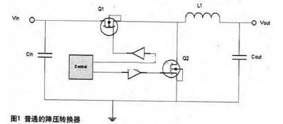
Although the principles discussed in this article are applicable to a wide range of power supply designs, we only focus on DC-to-DC converters. Because of its wide range of applications, almost every hardware engineer will be exposed to work related to it, maybe When must a power converter be designed. In this article, we will consider two common compromises related to low electromagnetic interference design; thermal performance, electromagnetic interference, and the size of the solution related to PCB layout and electromagnetic interference. In this article, we will use a simple step-down converter as an example, as shown in Figure 1.
Figure 1. Common step-down converter

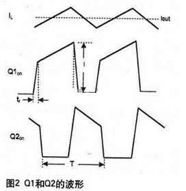
To measure radiated and conducted electromagnetic interference in the frequency domain, this is the Fourier series expansion of known waveforms. In this article, we focus on the performance of radiated electromagnetic interference. In a synchronous buck converter, the main switching waveforms that cause electromagnetic interference are generated by Q1 and Q2, that is, the current di/dt of each FET from the drain to the source during its respective conduction period. Figure The current waveforms (Q and Q2on) shown in 2 are not very regular trapezoids, but we have greater freedom of operation, because the transition of conductor current is relatively slow, so you can apply Henry Ott’s classic book "Electronic System Formula 1 in Noise Reduction Technology. We found that for a similar waveform, its rise and fall times will directly affect the harmonic amplitude or Fourier coefficient (In).

Figure 2. Waveforms of Q1 and Q2
In=2IdSin(nπd)/nπd *Sin(nπtr/T)/nπtr/T (1)
Among them, n is the harmonic order, T is the period, I is the peak current intensity of the waveform, d is the duty cycle, and tr is the minimum value of tr or tf.
In practical applications, it is very likely that odd and even harmonic emissions will be encountered at the same time. If only odd harmonics are generated, then the duty cycle of the waveform must be accurate to 50%. In practice, there are very few such duty cycle accuracy.

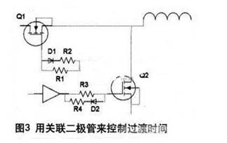
The electromagnetic interference amplitude of the harmonic series is affected by the on-off of Q1 and Q2. This can be clearly seen when measuring the rise time tr and fall time tf of the drain-source voltage VDS, or the rise rate di/dt of the current flowing through Q1 and Q2. This also means that we can reduce the level of electromagnetic interference simply by slowing down the on-off speed of Q1 or Q2. This is the case. Extending the switching time does have a great impact on harmonics with frequencies higher than f=1/πtr. However, at this time, a compromise must be made between increasing heat dissipation and reducing losses. Nevertheless, it is still a good way to control these parameters, it helps to strike a balance between electromagnetic interference and thermal performance. Specifically, it can be achieved by adding a small resistance resistor (usually less than 5Ω). This resistor can be connected in series with the gates of Q1 and Q2 to control tr and tf. You can also connect a "shut-off diode" in series to the gate resistor to control independently Transition time tr or tf (see Figure 3). This is actually an iterative process, even the most experienced power supply designers use this method. Our ultimate goal is to reduce the electromagnetic interference to an acceptable level by slowing down the transistor's turn-on and turn-off speed, while ensuring its temperature is low enough to ensure stability.
The above is an introduction to the PCB layout design scheme with low electromagnetic interference in the power module. Ipcb is also provided to PCB manufacturers and PCB manufacturing technology