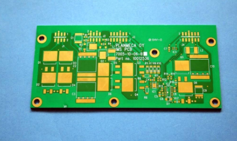
1.Side button, TP, screen, earphone, DC, battery, USB and other connectors should be sorted out as soon as possible to prevent errors.
2.All connectors such as screens, cameras, touch screens, etc. are easy to reverse in direction. When changing layers, the connectors must be changed 180 degrees.
3. If you put parts on the first floor, the second floor is the main ground, and the third floor is the copper layer for the power supply. The line is first completed on the surface layer, and the rest go to the third layer, and finally the second layer. The principle of the layer is to ensure the power supply The copper and the ground are intact, and the wiring in the middle of the second layer should be avoided as much as possible.

4, DC-DC circuit unit, the components of each unit are placed on the same side; the input first passes through the capacitor, the output capacitor is close to the inductor, the feedback loop is far away from the inductor to prevent interference, and the input and output filter capacitors are directly connected to the IC ground wire.
5. The output line of the audio power amplifier needs to be well isolated to prevent interference with other circuits.
6, NAND FLASH has a great opportunity to be welded by hand, small parts need to be avoided, and two short-circuit test points are left in the data line.
7. The audio decoder chip is difficult to solder according to the recommended package, and the length of the 0.2MM pad needs to be increased.
8, DC-DC circuit unit, the components of each unit are placed on the same side; the input first passes through the capacitor, the output capacitor is close to the inductor, the feedback loop is far away from the inductor to prevent interference, and the input and output filter capacitors are directly connected to the IC ground wire.
9.The signal frequency of HDMI will reach more than 100M, the signal difference should be handled well, and the signal processing chip and the connector should be placed on the same side as possible.
10.The side button fixed foot pad is easy to fall off and needs to be copper reinforced.
11.The device silk screen is divided into two layers, some are on the top layer, and some are on the bottom layer. They must be unified to prevent the silk screen from being missed.
The above is an introduction to the key points of tablet PC PCB design. Ipcb is also provided to PCB manufacturers and PCB manufacturing technology