DFM (Design for manufacturability) is design for manufacturing, and it is the core technology of concurrent engineering. Design and manufacturing are the two most important links in the product life cycle. Concurrent engineering is to consider factors such as product manufacturability and assemblability at the beginning of the design. So DFM is the most important support tool in concurrent engineering. Its key is the processability analysis of design information, the evaluation of manufacturing rationality and the suggestions for improving the design. In this article, we will briefly introduce the DFM general technical requirements in the PCB process.
Wanlong Lean provides intelligent manufacturing services such as PCB design, PCB board production proofing, SMT chip processing, circuit board welding, PCBA processing, PCBA foundry and other materials.
Summary of PCB design process DFM technical requirements
1. General requirements

1. As a general requirement for PCB design, this standard regulates PCB design and manufacturing and realizes effective communication between CAD and CAM.
2. When processing documents, our company will give priority to design drawings and documents as the production basis.
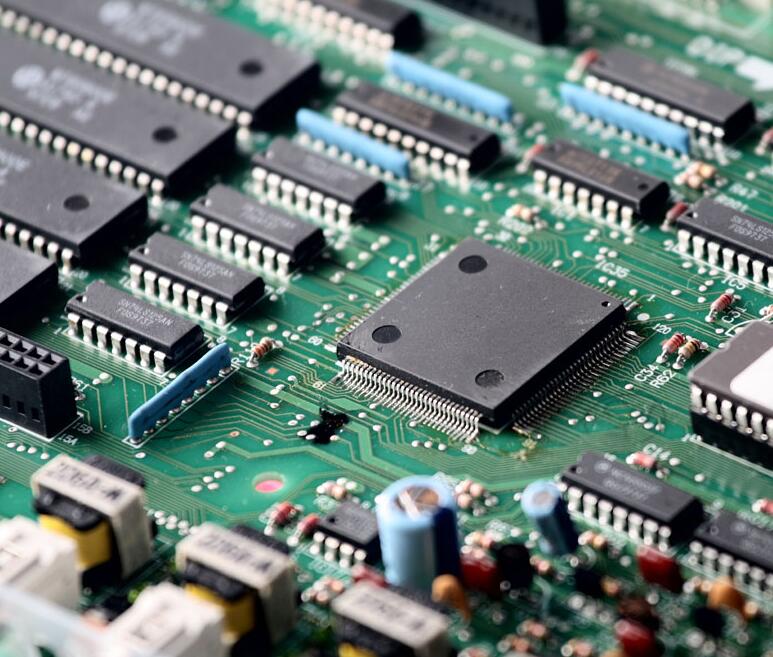
2. PCB material
1. Substrate
The substrate of PCB generally adopts epoxy glass cloth copper clad laminate, namely FR4. (Including single panel)
2. Copper foil
a) More than 99.9% electrolytic copper;
b) The thickness of copper foil on the surface of the finished double-layer board is ≥35?m (1OZ); when there are special requirements, specify in the drawings or documents.
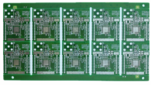
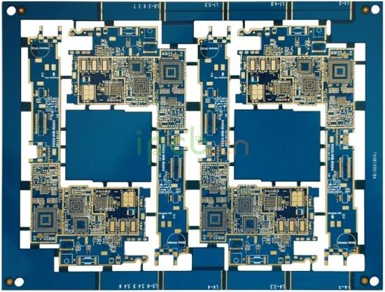
3. PCB structure, dimensions and tolerances
1. Structure
a) All relevant design elements that make up the PCB should be described in the design drawings. The appearance should be uniformly represented by Mechanical 1 layer (priority) or Keep out layer. If it is used in the design file at the same time, generally keep out layer is used for shielding, without opening holes, and using mechanical 1 for forming.
b) In the design drawing, it means to open a long slot hole or hollow out, and use the Mechanical 1 layer to draw the corresponding shape.
2. Board thickness tolerance
3. Overall dimension tolerance
The external dimensions of the PCB should conform to the requirements of the design drawings. When the drawing is not specified, the tolerance of the external dimension is ±0.2mm. (Except for V-CUT products)
4. Flatness (warpage) tolerance
The flatness of the PCB should meet the requirements of the design drawings. When the drawing is not specified, follow the instructions below
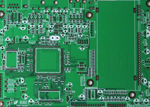
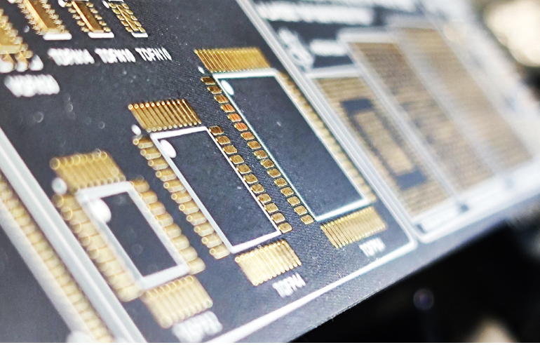
Four, printed wires and pads
1. PCB layout
a) In principle, the layout, line width and line spacing of printed wires and pads shall be in accordance with the design drawings. However, our company will deal with the following: appropriately compensate the line width and PAD ring width according to the process requirements. In general, our company will try to increase the PAD as much as possible for the single panel to enhance the reliability of customer welding.
b) When the design line spacing does not meet the process requirements (too dense may affect performance and manufacturability), our company will make appropriate adjustments according to the pre-manufacturing design specifications.
c) In principle, PCB company recommends that when designing single and double panels, the inner diameter of the via (VIA) should be set to 0.3mm or more, the outer diameter should be set to 0.7mm or more, the line spacing should be 8mil, and the line width should be 8mil or more. In order to reduce the production cycle to the greatest extent, reduce the manufacturing difficulty.
d) The minimum drilling tool of our company is 0.3, and the finished hole is about 0.15mm. The minimum line spacing is 6mil. The thinnest line width is 6mil. (But the manufacturing cycle is longer and the cost is higher)
2. Wire width tolerance
The internal control standard for the width tolerance of printed wires is ±15%
3. Grid processing
a) In order to avoid blistering on the copper surface during wave soldering and PCB bending due to thermal stress after heating, it is recommended to lay the large copper surface in a grid pattern.
b) The grid spacing is greater than or equal to 10mil (not less than 8mil), and the grid line width is greater than or equal to 10mil (not less than 8mil).
4. Treatment of thermal pad
In large-area grounding (electricity), the legs of components are often connected to it. The treatment of the connecting legs takes into account the electrical performance and process requirements. The possibility of excessively dispersing heat and producing virtual solder joints is greatly reduced.