The rapid development of the electronic information industry has enabled electronic products to develop in the direction of miniaturization, functionalization, high performance, and high reliability. From the general surface mount technology (SMT) in the mid-1970s to the high-density interconnect surface mount technology (HDI) in the 1990s, as well as the application of various new packaging technologies such as semiconductor packaging and IC packaging technology that have emerged in recent years, Electronic installation technology continues to develop in the direction of high density. At the same time, the development of high-density interconnect technology promotes the development of PCBs in the direction of high density. With the development of mounting technology and PCB technology, the technology of copper clad laminate as a PCB substrate material is also constantly improving.
Experts predict that the world's electronic information industry will grow at an average annual growth rate of 7.4% in the next 10 years. By 2020, the world's electronic information industry market will reach 6.4 trillion U.S. dollars, of which electronic complete machines will be 3.2 trillion U.S. dollars, and communication equipment and computers will account for More than 70% of them amounted to US$0.96 trillion. It can be seen that the huge market for copper clad laminates as electronic basic materials will not only continue to exist, but also continue to develop at a growth rate of 15%. The relevant information released by the Copper Clad Laminate Industry Association shows that in the next five years, in order to adapt to the development trends of high-density BGA technology and semiconductor packaging technology, the proportion of high-performance thin FR-4 and high-performance resin substrates will increase.

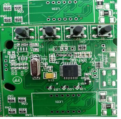
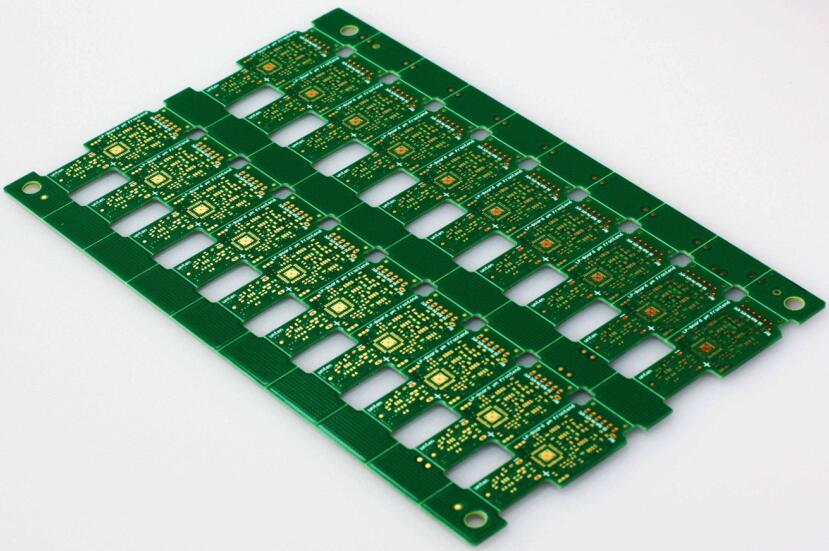
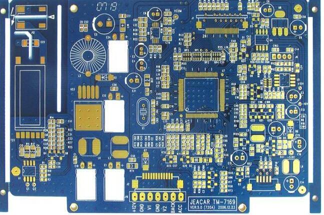
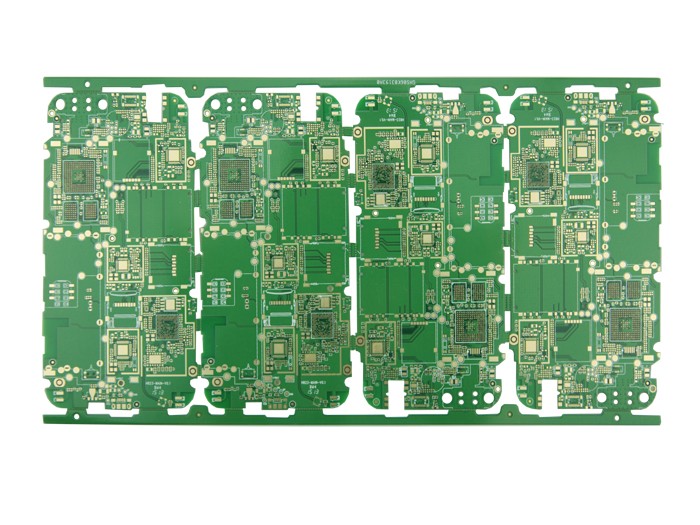
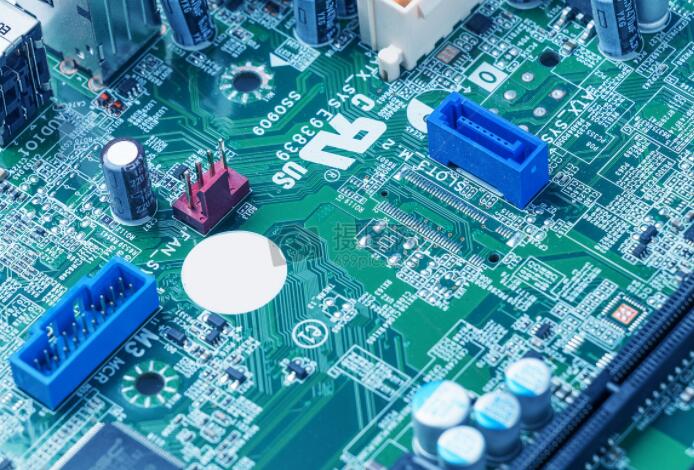
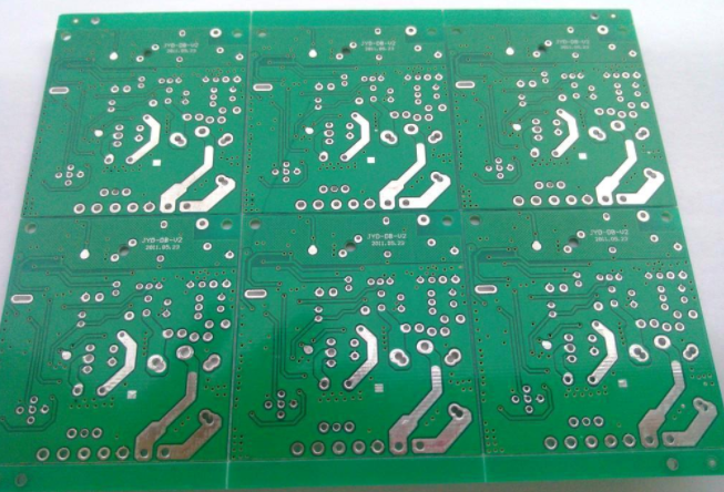
Copper Clad Laminate (CCL), as the substrate material in PCB manufacturing, mainly plays the role of interconnection, insulation and support to the PCB, and has a great impact on the transmission speed, energy loss, and characteristic impedance of the signal in the circuit. Therefore, the PCB The performance, quality, processability in manufacturing, manufacturing level, manufacturing cost, and long-term reliability and stability of CCL depend to a large extent on the material of the copper clad laminate.
1. PCB substrate material-lead-free compatible copper clad laminate
At the EU meeting on October 11, 2002, two "European Directives" with environmental protection content were passed. They will formally implement the resolution on July 1, 2006. The two "European Directives" refer to the "Electrical and Electronic Product Waste Directive" (referred to as WEEE) and the "Restriction of the Use of Certain Hazardous Substances" (referred to as RoHs). In these two statutory directives, the requirements are clearly mentioned. The use of lead-containing materials is prohibited. Therefore, the best way to respond to these two directives is to develop lead-free copper clad laminates as soon as possible.
2. PCB substrate material-high performance copper clad laminate
The high-performance copper clad laminates referred to here include low dielectric constant (Dk) copper clad laminates, copper clad laminates for high frequency and high speed PCBs, high heat resistance copper clad laminates, and various substrate materials for multi-layer laminates (resin coated copper Foil, organic resin film that constitutes the insulating layer of laminated multilayer board, glass fiber reinforced or other organic fiber reinforced prepreg, etc.). In the next few years (to 2010), in the development of this type of high-performance copper clad laminates, according to the forecasted future development of electronic installation technology, the corresponding performance index values should be reached.
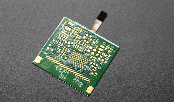
3. PCB substrate material-substrate material for IC package carrier board
The development of substrate materials for IC packaging substrates (also known as IC packaging substrates) is currently a very important topic. It is also an urgent need to develop China's IC packaging and microelectronics technology. With the development of IC packaging in the direction of high frequency and low power consumption, IC packaging substrates will be improved in important properties such as low dielectric constant, low dielectric loss factor, and high thermal conductivity. An important subject of future research and development is the effective thermal coordination and integration of substrate thermal connection technology-heat dissipation.
In order to adapt to the development of high speed, the dielectric constant of the substrate should reach 2.0, and the dielectric loss factor can be close to 0.001. For this reason, a new generation of printed circuit boards that exceed the boundaries of traditional substrate materials and traditional manufacturing processes are predicted to appear in the world around 2005. The breakthrough in technology, first of all, is the breakthrough in the use of new substrate materials.
To predict the future development of IC packaging design and manufacturing technology, there are more stringent requirements for the substrate materials used in it. This is mainly manifested in the following aspects:
1. High Tg corresponding to lead-free solder.
2. Achieve low dielectric loss factor matching the characteristic impedance.
3. Low dielectric constant corresponding to high speed (ε should be close to 2).
4. Low warpage (improve the flatness of the substrate surface).
5. Low moisture absorption rate.
6. Low thermal expansion coefficient, so that the thermal expansion coefficient is close to 6ppm.
7. Low cost of IC package carrier.
8. Low-cost substrate material with built-in components.
9. In order to improve the thermal shock resistance, the basic mechanical strength is improved. It is suitable for the substrate material that does not reduce the performance under the temperature change cycle from high to low.
10. A low-cost green substrate material suitable for high reflow soldering temperature.
Four, PCB substrate material has a copper clad laminate with special functions
The copper clad laminates with special functions referred to here mainly refer to: metal-based (core) copper clad laminates, ceramic-based copper clad laminates, high-dielectric constant laminates, copper clad laminates (or substrate materials) for embedded passive component-type multilayer boards, Copper-clad laminates for optical-electric circuit substrates, etc. The development and production of this type of copper clad laminate is not only required for the development of new technologies for electronic information products, but also for the development of China's aerospace and military industries.
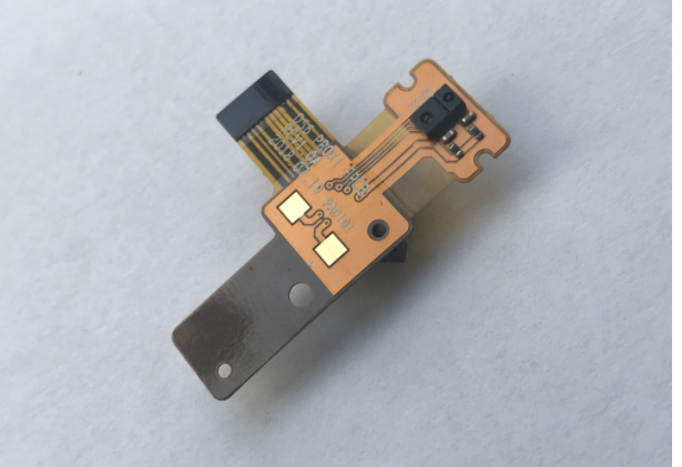
Five, PCB substrate material high-performance flexible copper clad laminate
In terms of flexible copper clad laminates, there is a big gap between China and advanced countries and regions in the production scale, manufacturing technology level and raw material manufacturing technology, and this gap is even greater than that of rigid copper clad laminates.
Summarize
The development of copper clad laminate technology and production and the electronic information industry, especially the development of the PCB industry are synchronized and inseparable. This is a process of continuous innovation and continuous pursuit. The progress and development of copper clad laminates are also driven by the innovation and development of electronic products, semiconductor manufacturing technology, electronic mounting technology, and PCB manufacturing technology. In this case, we will make progress together., Synchronous development is particularly important.