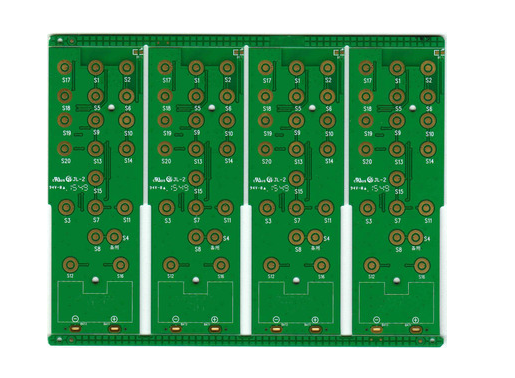
Features of PCBA surface mount printed boards
The printed circuit boards used for the mounting and interconnection of electronic components must adapt to the rapid development of the current surface mount technology (PCBA processing). Surface-mounted printed boards (SMB) include simpler single-sided boards, more complex double-sided printed boards, as well as multi-layer boards that are more difficult and more complex in PCBA processing.
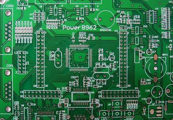
In the 1990s, the international PCB technology was reformed and developed with the goal of being able to produce higher and higher density SMBs. SMB has become the mainstream product of current advanced PCB manufacturers, and almost 100% of PCBs are SMB. The surface-mounted printed board has the following main features compared with the printed board where the lead components are inserted.
After using surface-mounted components and devices, the metallized holes on the printed circuit board are no longer used for inserting components and device leads, and soldering is no longer carried out in the metallized holes. The metallized holes are only used for electrical interconnection. Minimize the aperture as much as possible, from 0.5-1.0mm in the past to 0.3, 0.2 or 0.1mm. Foreign countries call the aperture of 0.3-0.5mm a small hole (Small Hole), which will be smaller than 0.3mm. The holes in the SMB are mainly micro-holes and small holes. It is estimated that the small holes with a diameter of less than 0.48mm accounted for only 5% in 1984 and increased to 31% in 1991.
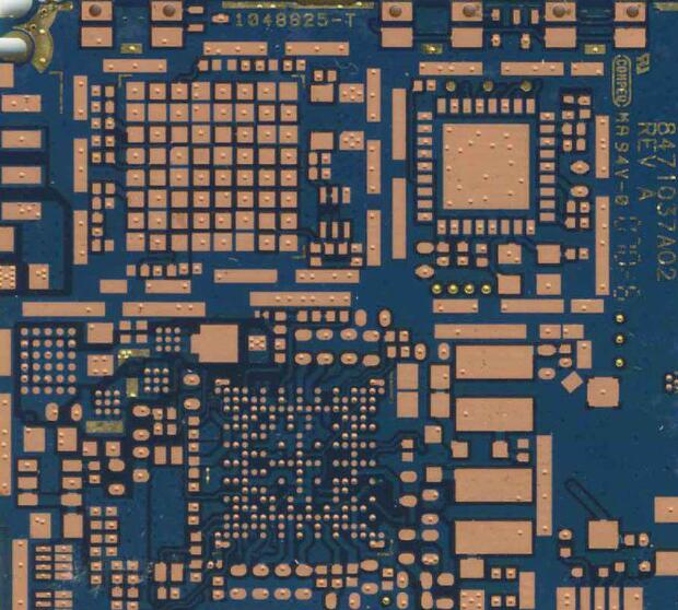
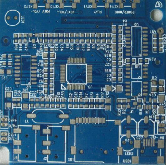
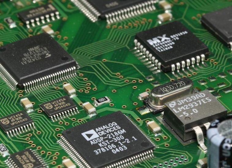
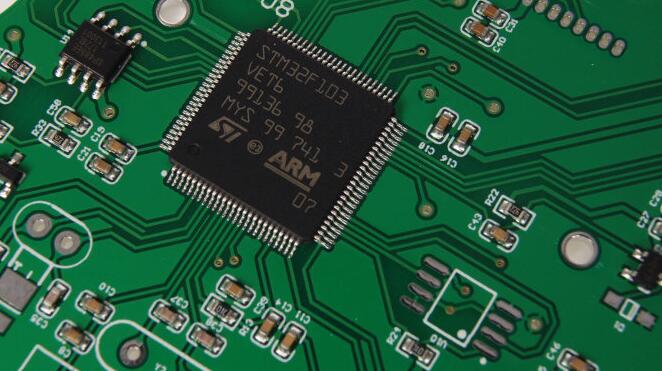
The number of IC pins for PCBA processing is as high as 100 to 500, and the number of MCM components is as high as 1000-2000. The pin center distance has been reduced from 2.54mm to 1.27, 0.635, O. 3175mm, and even O.15mm., SMB requires fine lines and narrow spacing, and the line width is reduced from 0.2-O.3mm to O.15mm, O.10mm, or even 0.05mm. From the past two wires placed between two pads increased to 3-5 wires. For such a thin wire, it is extremely difficult to visually check for gaps, short circuits, and open circuits. It is estimated that thin wires with a width of less than 0.13 mm accounted for only 4% in 1984, and it increased to 28 in 1992. %.

Since surface mount components are to be mounted on the SMB, high accuracy of the wire pattern is required, especially the land pattern accuracy requires +/-O.05mm, and the positioning accuracy requires +/-O.05-0.075mm.
Due to fine lines and high precision, the requirements for the surface defects of the substrate are strict, especially for the flatness of the substrate. The warpage of SMB is required to be controlled within 0.5%, while the warpage of general non-SMB printed boards is required to be less than l-1.5%.
The dimensional stability of SMB is required to be good, and the thermal expansion coefficient of the mounted leadless chip carrier and the substrate material should be matched, so as to avoid the stress caused by the different thermal expansion value in the harsh environment causing the lead to break. Quartz fiber base, BT resin, PI resin copper clad substrate, copper/invar/copper metal core substrate material can be used in strict environment.
SMB requires a smooth metal plating (coating) coating on the pad. PCBA processed tin-lead alloy electroplated printed boards that are hot melted are generally arc-shaped surfaces due to the surface tension of the tin-lead alloy during the hot melt process. It is not conducive to the accurate positioning and placement of SMD, vertical hot air leveling solder-coated printed boards, due to the effect of gravity, the lower part of the pad is generally protruding than the upper part, not flat enough, and it is not conducive to mounting SMD, and vertical hot air leveling Flat printed boards are not evenly heated, and the lower part of the board takes longer to heat up than the upper part, which is prone to warping. Therefore, SMB should not use hot-melt tin-lead alloy coating and vertical hot-air leveling solder coating. Horizontal type is required. Hot air leveling technology or other plating (coating) technology. Water-soluble heat-resistant pre-solder has been used to replace the hot air leveling process.
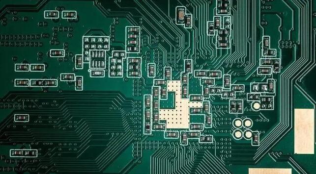
The solder mask on SMB also requires high precision. The commonly used method of screen printing solder mask is difficult to meet the high precision requirements. Therefore, the solder mask on SMB is mostly made of liquid photosensitive solder resist for PCBA processing. SMD can be installed on both sides, so SMB also requires solder mask graphics and marking symbols to be printed on both sides of the board.
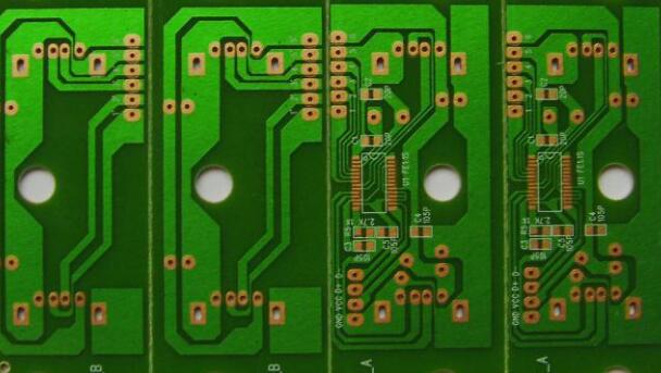
When installing SMD on PCBA processing SMB, mounters are used. Most of them use large imposition for surface mounting. After infrared welding or vapor phase welding, the SMB is separated one by one. Therefore, SMB is required to be supplied in the form of large imposition. Use V-groove milling or milling grooves to leave nodes.
High-density multilayer SMBs mostly use blind and buried via technologies. In addition to 90-degree wiring, 45-degree diagonal wiring is also used in the design. Buried vias are plated holes that connect two or more inner layers in the multilayer board. Blind vias are used to connect the outer layer of the multilayer board with one or more inner layer-oriented plating holes. The use of buried vias and blind vias is an effective method to improve the wiring density of the multilayer board, reduce the number of layers and the board size, and can greatly reduce The number of through-plated holes.
PCBA processing and mounting of SMBs with high-speed circuits requires control of characteristic impedance, and the use of thinner materials to develop thinner.