Electrical design factors of resistor/capacitor in PCBA patch processing
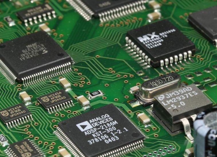
1, PCBA chip processing resistance
Usually the current carrying capacity of the wire is not a problem; but when the wire is very long and the voltage regulation requirements are very strict, the ohmic resistance may be a problem. The resistance value and temperature rise of the wire can be calculated approximately from Figure 1.16. The resistance value and temperature can also be calculated by the following formula:
R=0.000227W
In the formula, R is the resistance value per inch of wire length, measured in ohms; W is the width of the wire, measured in inches; it is calculated on the basis that the minimum purity of copper is 99.5% and the thickness of copper is 0.0027 inches (2 ounces). of.
2, PCBA chip processing line capacitance
Capacitance may be quite important, especially in the high-frequency range. When it comes to high-frequency circuits, the distributed capacitance between one wire and the other wire must be considered; it is about 1 picofarad/ft. As an approximate guide. The following basic capacitance formula can be used:

Formula 1
When the wire width is at least 10 times the dielectric spacing, generally speaking, the formula is basically the same as the actual measured value. PCBA patch processing but the calculated value may be a little lower. The coupling capacitance between wires can be minimized by limiting the wiring length of the wires on the same horizontal plane. The capacitance between adjacent wires is a function of wire width, thickness, spacing and the characteristics of the sheet itself, which can be calculated as follows:
formula 2
Where: K = dielectric constant of the base; a = wire thickness (inch); b = wire width (inch); d = distance between wires (inch)
Special attention must be paid to the circuit located on the shielding surface or the grounding surface, because the entire wire length combined with the shielding or grounding surface forms a capacitance, and the combination of some similar wires in the same situation will inevitably form a capacitance.
PCBA patch processing has pointed out: For key high-value circuits, the electrical characteristics of single-sided printed circuits made of 1/16 inch epoxy-glass or epoxy paper are not enough, and they must be connected to the ground plane. The microstrip wire structure. Electrical characteristics can also be used as a process control method, which can clearly indicate the amount of process parameters. iPCB is happy to be your business partner. Our business goal is to become the most professional prototyping PCB manufacturer in the world. With more than ten years of experience in this field, we are committed to meeting the needs of customers from different industries in terms of quality, delivery, cost-effectiveness and any other demanding requirements. As one of the most experienced PCB manufacturers and SMT assemblers in China, we are proud to be your best business partner and good friend in all aspects of your PCB needs. We strive to make your research and development work easy and worry-free.
quality assurance
iPCB has passed ISO9001:2008, ISO14001, UL, CQC and other quality management system certifications, produces standardized and qualified PCB products, masters complex process technology, and uses professional equipment such as AOI and Flying Probe to control production and X-ray inspection machines. Finally, we will use double FQC inspection of appearance to ensure shipment under IPC II standard or IPC III standard.