What are the instructions for the appearance inspection of PCBA processing?
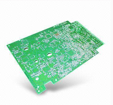
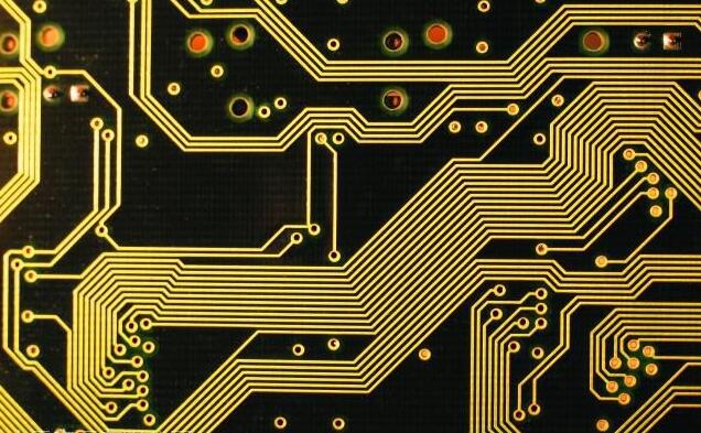
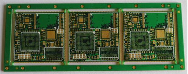
Shenzhen PCBA processing printed circuit boards, also known as printed circuit boards, printed circuit boards, often use the English abbreviation PCBA, which is an important electronic component, a support for electronic components, and a provider of circuit connections for electronic components. Because it is made using electronic printing technology, it is called a "printed" circuit board. Before the advent of printed circuit boards, the interconnection between electronic components relied on the direct connection of wires to form a complete circuit.
Now, the circuit breadboard only exists as an effective experimental tool, and the printed circuit board has become an absolute dominant position in the electronics industry. But most people still don't know what the PCBA processing appearance inspection instructions are. Let's take a look at the editor of Shenzhen PCBA processing.
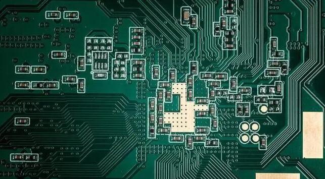
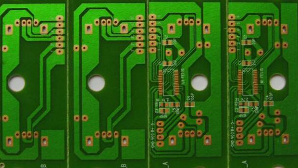
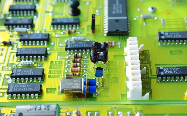
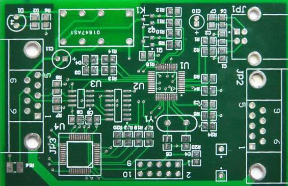
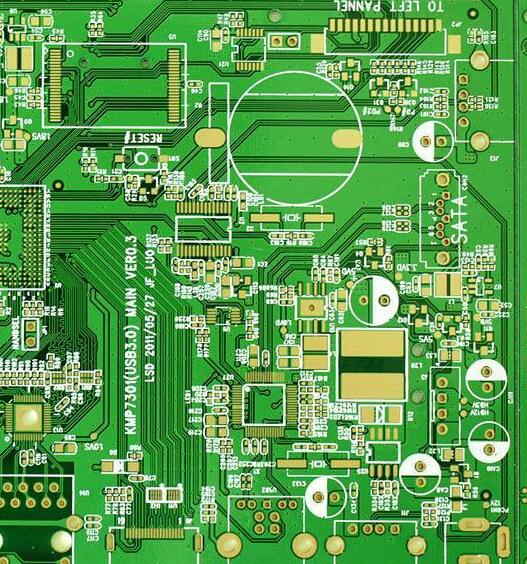
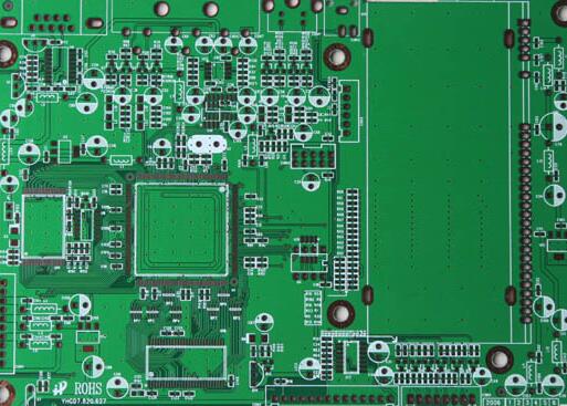
Shenzhen PCBA processing appearance inspection instructions:
Missing parts: The components are not mounted as required in the corresponding position on the PCBA.
Empty soldering: 3/4 of the area of the solder joint without or less soldering on the component feet (for patch components, the soldering area is less than 1/2 of the width of the component).
Tin connection: Due to abnormal operation, the two points that were originally electrically unconnected were connected with tin.
Wrong parts: The components mounted on the PCBA do not match those shown on the BOM
Dummy soldering: The component pins are not well tinned, and effective soldering cannot be guaranteed (including fake soldering)
Cold welding: The surface of the solder joint is gray without good wetting.

Reverse: The polarity after the component is mounted is opposite to that specified in the document
tombstone: One end of the patch component is lifted away from the pad to form a tombstone
Reverse back: The front of the module (the silk-screened surface) is facing down, but the welding is normal
Open circuit: The component pin is disconnected or the circuit on the PCBA board is disconnected
tombstone: One end of the patch component is lifted away from the pad to form a tombstone
Reverse back: The front of the module (the silk-screened surface) is facing down, but the welding is normal
Open circuit: The component pin is disconnected or the circuit on the PCBA board is disconnected
Lifting: The copper foil or pad of the circuit is lifted out of the PCBA surface and exceeds the specification
Multiple pieces: The file indicates the position of no components, and there are components on the corresponding PCBA board
Tin crack: Usually after the solder joint is subjected to external force, the solder joint and the component pin are separated, which affects the soldering effect or has hidden dangers
At present, the country has higher and higher requirements for environmental protection and greater efforts in link governance. This is a challenge but also an opportunity for PCB factories. If PCB factories are determined to solve the problem of environmental pollution, then FPC flexible circuit board products can be at the forefront of the market, and PCB factories can get opportunities for further development.
We provide one-stop service for PCBA processing, full BOM component purchasing, PCBA model placement. Mainly based on PCBA model patch and batch SMT processing, providing PCBA sample soldering, sample processing, circuit board soldering, BGA soldering, BGA ball planting, BGA packaging processing, BGA flying leads, SMT patch processing, SMT foundry, OEM, etc. service.