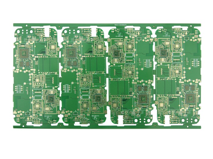
Basic procedure of PCB failure analysis

To obtain the exact cause or mechanism of PCB failure or failure, the basic principles and analysis process must be followed, otherwise valuable failure information may be missed, causing the analysis to be unable to continue or may get wrong conclusions. The general basic process is that, first, based on the failure phenomenon, the failure location and failure mode must be determined through information collection, functional testing, electrical performance testing, and simple visual inspection, that is, failure location or failure location. For simple PCB board or PCBA, the failure location is easy to determine, but for more complex BGA or MCM packaged devices or substrates, the defects are not easy to observe through a microscope and are not easy to determine for a while. At this time, other means are needed to determine. Then we must analyze the failure mechanism, that is, use various physical and chemical methods to analyze the mechanism that causes PCB failure or defect generation, such as virtual welding, pollution, mechanical damage, moisture stress, medium corrosion, fatigue damage, CAF or ion migration, Stress overload and so on. Then there is the failure cause analysis, that is, based on the failure mechanism and process analysis, to find the cause of the failure mechanism, and test verification if necessary. Generally, test verification should be performed as much as possible, and the accurate cause of induced failure can be found through test verification. This provides a targeted basis for the next improvement. Finally, it is to compile a failure analysis report based on the test data, facts and conclusions obtained in the analysis process, requiring clear facts, strict logical reasoning, and strong organization. Do not imagine out of thin air.
In the process of analysis, pay attention to the basic principles that the analytical method should be used from simple to complex, from outside to inside, never destroying the sample and then using it. Only in this way can we avoid the loss of key information and the introduction of new man-made failure mechanisms. It is like a traffic accident. If the party involved in the accident destroys or escapes the scene, it is difficult for the wise police to make an accurate determination of responsibility. At this time, the traffic laws generally require the person who fled the scene or the party who destroyed the scene to bear full responsibility. The failure analysis of PCB or PCBA is the same. If you use an electric soldering iron to repair the failed solder joints or use large scissors to forcefully cut the PCB, then there is no way to start the analysis, and the failure site has been destroyed. Especially when there are few failed samples, once the environment of the failure site is destroyed or damaged, the real failure cause cannot be obtained.
The above is an introduction to the basic procedures of PCB failure analysis. Ipcb is also provided to PCB manufacturers and PCB manufacturing technology