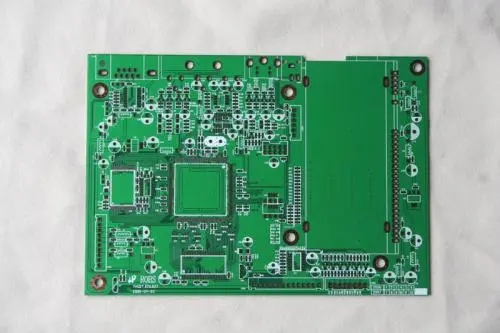
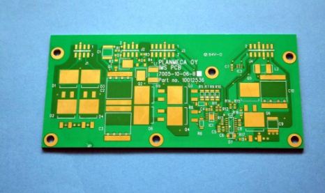
1. Commonly used Stackup:
Eight-layer board
L1-TOP
L2-GND
L3-SIG
L4-SIG
L5-PWR
L6-SIG
L7-GND
L8-BOT
Six-layer board
L1-TOP
L2-SIG
L3-GND
L4-SIG
L5-PWR
L6-BOT

2. Each layer routing strategy: Try to arrange the high data rate bus data bus such as SDRAM DATA and ADDRESS bus, LCD DATA bus, SD card DATA line to the layer near the main ground layer, preferably upper and lower layers Shielded by the ground.
3. The principle of power supply wiring: the current flow direction is guaranteed to go to the decoupling capacitor and then to the IC pin; star wiring, that is, when a power supply supplies power to multiple modules, pay attention to the bus width is large enough, one branch to one module or They are circuits of the same nature and should not be connected in series. The power supply of high-frequency modules such as FM transmitter modules, GPS, and Bluetooth modules should be branched from a relatively clean (or power source end) bus node and then to each module; the charging part and For battery power supply, the current of the USB power supply part is relatively large, and the line width is required to be more than 40mils. The large-capacity filter capacitor is grounded nearby and connected to the main ground with more VIA.
4. Try to put the traces on the side of the board to the inner layer, and the ground pads of the components on the side of the board are facing the side of the board.
5. Each circuit module is shielded by a shielding cover. The width of the bare copper corresponding to the shielding cover is about 40mil (1mm). The shielding cover adopts serrated pads for easy soldering. The distance between the component and the shield is at least about 12 mils.
6. Every 2 to 3 ground pins in the BGA are connected to the main ground via a via hole, and the power pin is the same. All IC and BGA surface layers with heat-dissipating copper need to add KEEPOUT to prevent copper and plane from entering.
7. The length of the DATA bus and the ADDRESS bus of the SDRAM are approximately the same. The clock line to the CPU must first come out of the CPU (BGA) and then to the two SDRAMs respectively, to ensure that the distance to the SDRAM remains the same.
8. The copper sheets of each layer under the Bluetooth and GPS antennas need to be hollowed out, and other signals should be far away from the RF impedance control line; all grounding pads should be provided with grounding vias nearby.
9. The shortest path of crystal oscillator output enters RFRECIEVER, the line width is 4mil, and part of the surface of the RF module is hollowed out.
10. GPS_RF_CLK, GPS_DATA1, GPS_DATA2 should be wired as short as possible, and they should be ground-wrapped, at least three sides are ground-wrapped, and the fourth side has only small signal lines and vertical, and there must be no large signal lines without ground plane isolation.
11. SPEAKER output line differential, try to cover the ground, line width at least 12mil, try to achieve 16mil; Mic, micbias line differential, try to cover the ground, line width at least 8mil; earphone audio signal try to cover the ground, line width at least 12mil; audio AUDIOPA The output line is differential output, the line width is at least 12mil.
12. Analog signal lines such as ADC (such as touch screen position control signals tspx, tspy, tsmx, tsmy) go through the analog layer, and try to cover the ground or be close to the ground.
13. The crystal (crystal oscillator) corresponds to the hollowing out of the bottom layer, and no other signal lines can pass through this layer.
14. BGA LAYOUT self summary:
A Wiring sequence: ground wire power line punching-SDRAM-Flash-LCD-SD card-GPS-Allclock&resetsignals-AC97CODE-BT-FM-Otherpart
bBGA outer two circles of pins are directly drawn from the surface layer to connect with other components or punched to go to the inner layer, and the pins above the third circle are punched radially and then go to the inner layer.
C The fan-out sequence of the signal lines connected to the BGA in the way of exclusion and exclusion follows the exclusion and capacitance.
The signal line fan-out sequence of dSDRAM follows SDRAM.
The above is the introduction of GPS PCB design experience summary, Ipcb also provides PCB manufacturers and PCB manufacturing technology