Electromagnetic compatibility in PCB printed circuit board(PCB) development technology
Electromagnetic compatibility (EMC, Electromagnetic Compatibility) refers to the ability of electronic equipment to work in a coordinated and effective manner in various electromagnetic environments. The purpose of electromagnetic compatibility design is to enable electronic equipment to suppress all kinds of external interference, so that the electronic equipment can work normally in a specific electromagnetic environment, and at the same time to reduce the electromagnetic interference of the electronic equipment itself to other electronic equipment. The electromagnetic compatibility in PCB design involves many factors. The following will mainly explain from three parts, and the specific selection should integrate various factors.

A The overall layout of the printed circuit board and device layout
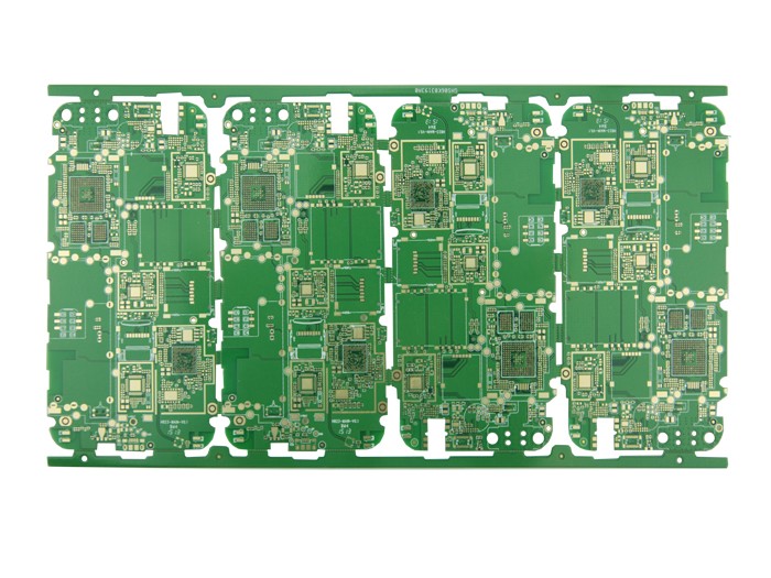
1. The success of a product depends on the internal quality and the overall aesthetics. Only when both are perfect can the product be considered successful; on a PCB board, the layout requirements of the components must be balanced and sparse. Dense and orderly, not top-heavy or heavy, with as few vias as possible; the best shape of the circuit board is rectangular. The aspect ratio is 3:2 or 4:3; 4-layer board has 20dB lower noise than double-sided board. 6-layer board has 10dB lower noise than 4-layer board. Try to use multilayer board when economic conditions permit.
2. The circuit board is generally divided into analog circuit area (for fear of interference), digital circuit area (for fear of interference and interference), and power drive area (interference source), so the board should be divided into three areas reasonably.
3. Generally, select devices with low power consumption and good stability, and use high-speed devices as little as possible.
4. The lines are exquisite: wide lines should never be thin if possible; high-voltage and high-frequency lines should be round and slippery, without sharp chamfers, and corners should not be at right angles. The ground wire should be as wide as possible, and it is best to use a large area of copper, which can greatly improve the problem of grounding points.
5. The external clock is a source of high-frequency noise. In addition to causing interference to the application system, it may also cause interference to the outside world, making the electromagnetic compatibility test fail to meet the standard. In application systems that require high system reliability, selecting a low-frequency microcontroller is one of the principles to reduce system noise. Taking the 8051 microcontroller as an example, the shortest instruction cycle is 1? When s, the external clock is 12MHz. And the Motorola MCU system clock of the same speed only needs 4MHz, which is more suitable for industrial control systems. In recent years, some manufacturers that produce 8051-compatible microcontrollers have also adopted some new technologies to reduce the demand for external clocks to 1/3 of the original without sacrificing computing speed. Motorola microcontrollers have introduced new 68HC08 series and its 16 /32-bit single-chip microcomputers generally use internal phase-locked loop technology to reduce the external clock frequency to 32KHz, while the internal bus speed is increased to 8MHz or even higher.
6. The wiring must have a reasonable direction: such as input/output, AC/DC, strong/weak signal, high frequency/low frequency, high voltage/low voltage, etc..., their directions should be linear (or separated), and they must not be mutually. blend. Its purpose is to prevent mutual interference. The best direction is in a straight line, but it is generally not easy to achieve, and the most unfavorable direction is a circle. For DC, small signal, low voltage PCB design requirements can be lower. So "reasonable" is relative. The routing direction between the upper and lower layers is basically vertical. The entire board does not want to be uniform, so don't squeeze it together.
7. As with other logic circuits in terms of device layout, the devices related to each other should be placed as close as possible so that a better anti-noise effect can be obtained. The clock generator, crystal oscillator, and the clock input of the CPU are all prone to noise. They should be close to each other, especially do not run signal lines under the crystal oscillator. It is very important that noise-prone devices, low-current circuits, and high-current circuits should be kept away from logic circuits as far as possible. If possible, separate circuit boards should be made.
B Ground wire technology SkE safety and electromagnetic compatibility network
1. Analog circuits and digital circuits have many similarities and differences in the design and wiring methods of component layouts. In the analog circuit, due to the existence of the amplifier, the very small noise voltage generated by the wiring will cause serious distortion of the output signal. In the digital circuit, the TTL noise tolerance is 0.4V ~ 0.6V, and the CMOS noise tolerance is 0.3 of Vcc. ~ 0.45 times, so the digital circuit has a strong anti-interference ability. The reasonable choice of a good power and ground bus mode is an important guarantee for the reliable operation of the instrument. Quite a lot of interference sources are generated through the power and ground bus, and the ground wire causes the greatest noise interference.
2. Separate the digital ground from the analog ground (or ground it at one point), and widen the ground wire. The width of the ground wire should be determined according to the current. Generally speaking, the thicker the better (the 100mil wire passes approximately 1 to 2A current). Ground wire>power wire>signal wire is a reasonable choice of line width.
3. The power line and the ground line should be as close as possible, and the power supply and the ground on the entire printed board should be distributed in a "well" shape in order to balance the distribution line current.
4. In order to reduce the crosstalk between the lines, if necessary, increase the distance between the printed lines, and insert some zero-volt lines as isolation between the lines. Especially between input and output signals, the three technologies of decoupling, filtering and isolation
1. Decoupling, filtering, and isolation are the three commonly used measures for hardware anti-interference.
2. Connect a 10~100uf electrolytic capacitor across the power input. If possible, it is better to connect to 100uF or more; in principle, each integrated circuit chip should be equipped with a 0.01pF ceramic capacitor, if the gap of the printed circuit board is not enough, 1~10pF can be arranged for every 4~8 chips But the capacitor; for devices with weak noise immunity and large power changes when turned off, such as RAM and ROM storage devices, the decoupling capacitor should be directly connected between the power line and the ground line of the chip;
3. Filtering refers to the classification of various signals according to frequency characteristics and control their direction. Commonly used are various low-pass filters, high-pass filters, and band-pass filters. The low-pass filter is used on the connected AC power line to allow 50-week AC power to pass smoothly and lead other high-frequency noises to the ground. The configuration index of the low-pass filter is the insertion loss. If the insertion loss of the selected low-pass filter is too low, it will not suppress the noise, and the too high insertion loss will cause "leakage" and affect the personal safety of the system. High-pass and band-pass filters should be selected and used according to the signal processing requirements in the system.
4. The typical signal isolation is photoelectric isolation. The use of photoelectric isolation devices to isolate the input and output of the single-chip microcomputer, on the one hand, prevents interference signals from entering the single-chip microcomputer system, and on the other hand, the noise of the single-chip microcomputer system itself will not spread out by conduction. Shielding is used to isolate the space radiation, and the parts with high noise, such as switching power supply, are covered with a metal box, which can reduce the interference of noise sources to the single-chip system. For analog circuits that are particularly afraid of interference, such as high-sensitivity weak signal amplifier circuits, they can be shielded. The important thing is that the metal shield itself must be connected to the real SkE safety and electromagnetic compatibility network.
The above is the introduction of electromagnetic compatibility in printed circuit board (PCB) development technology. Ipcb is also provided to PCB manufacturers and PCB manufacturing technology.