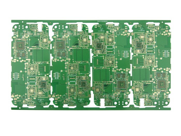
PCB design ground interference countermeasures

1. Ground loop countermeasures can be known from the mechanism of ground loop interference, as long as the current in the ground loop is reduced, the ground loop interference can be reduced. If the current in the ground loop can be completely eliminated, the problem of ground loop interference can be completely solved. Therefore, we propose the following solutions to ground loop interference.
A. Floating the equipment at one end If the circuit at one end is floated, the ground loop will be cut off, so the ground loop current can be eliminated. But there are two issues that need to be paid attention to. One is that for safety reasons, circuits are often not allowed to float. At this time, consider grounding the device through an inductor. In this way, for 50Hz AC current equipment, the grounding impedance is very small, and for higher frequency interference signals, the equipment grounding impedance is larger, which reduces the ground loop current. But doing so can only reduce the ground loop interference of high frequency interference. Another problem is that although the device is floating, there is still a parasitic capacitance between the device and the ground. This capacitance will provide a lower impedance at higher frequencies, so it cannot effectively reduce the high-frequency ground loop current.
B. Use a transformer to realize the connection between the devices. Use a magnetic circuit to connect the two devices to cut off the ground loop current. But it should be noted that the parasitic capacitance between the primary and secondary transformers can still provide a path for the higher frequency ground loop current, so the transformer isolation method has a poor suppression effect on the high frequency ground loop current. One way to improve the high-frequency isolation effect of the transformer is to install a shielding layer between the primary and secondary stages of the transformer. But it must be noted that the grounding end of the shielding layer of the isolation transformer must be at one end of the receiving circuit. Otherwise, not only cannot improve the high-frequency isolation effect, but also may make high-frequency coupling more serious. Therefore, the transformer should be installed on the side of the signal receiving device. A well-shielded transformer can provide effective isolation at frequencies below 1MHz.
C. Use an optical isolator to cut off the ground loop is to use light to achieve signal transmission. This can be said to be the most ideal way to solve the problem of ground loop interference. There are two methods for optical connection, one is optocoupler device, and the other is connection with optical fiber. The parasitic capacitance of the optocoupler is generally 2pf, which can provide good isolation at very high frequencies. Optical fiber has almost no parasitic capacitance, but it is inferior to optocoupler devices in terms of installation, maintenance, and cost.
D. Use of common mode chokes. Using common mode chokes on the connecting cable is equivalent to increasing the impedance of the ground loop, so that under a certain ground voltage, the ground loop current will decrease. But pay attention to control the parasitic capacitance of the common mode choke, otherwise the isolation effect on high frequency interference is very poor. The more turns of the common mode choke, the greater the parasitic capacitance and the worse the effect of high-frequency isolation.
2. Eliminate common impedance coupling
There are two ways to eliminate the common impedance coupling. One is to reduce the impedance of the common ground line, so that the voltage on the common ground line is also reduced, thereby controlling the common impedance coupling. Another method is to avoid the common grounding of circuits that are easy to interfere with each other through proper grounding. Generally, it is necessary to avoid the common grounding of high-current circuits and weak-current circuits, and the common grounding of digital circuits and analog circuits. As mentioned earlier, the core problem of reducing the impedance of the ground wire is to reduce the inductance of the ground wire. This includes using a flat conductor as the ground wire, and using multiple parallel conductors that are far apart as the ground wire. For printed circuit boards, laying a ground wire grid on a double-layer board can effectively reduce the ground wire impedance. In a multilayer board, a special layer of ground wire has a small impedance, but it will increase the cost of the circuit board. . The grounding method to avoid common impedance through proper grounding method is parallel single-point grounding, as shown in Figure 4. The disadvantage of parallel grounding is that there are too many grounded wires. Therefore, in practice, it is not necessary for all circuits to be connected in parallel with single-point grounding. For circuits with less mutual interference, single-point grounding in series can be used. For example, the circuits can be classified according to strong signals, weak signals, analog signals, digital signals, etc., and then use single-point grounding in series within similar circuits, and single-point grounding in parallel for circuits of different types.
The above is the introduction of PCB design ground interference countermeasures. Ipcb is also provided to PCB manufacturers and PCB manufacturing technology.