Wearable devices require high reliability, which can be a problem when PCB designers are faced with the choice of FR4 (the most cost-effective PCB manufacturing material) or more advanced and expensive materials.
Because of their small size and size, there are few ready-made printed circuit board standards for the growing wearable Internet of Things market. Prior to these standards, we had to rely on knowledge and manufacturing experience gained in board-level development and think about how to apply them to unique emerging challenges. There are three areas that require special attention: circuit board surface materials, RF/microwave design, and RF transmission lines.
PCBs generally consist of layers, which may be made of fibre reinforced epoxy resins (FR4), polyimides or Rogers or other laminates. Insulating materials between layers are called semicurable sheets.
Wearable devices require high reliability, which can be a problem when PCB designers are faced with the choice of FR4 (the most cost-effective PCB manufacturing material) or more advanced and expensive materials.
If wearable PCB applications require high-speed, high-frequency materials, FR4 may not be the best choice. The dielectric constant (Dk) of FR 4 is 4.5, that of the more advanced Rogers 4003 series is 3.55, and that of the brothers Rogers 4350 is 3.66.

Figure 1: A stacked diagram of a multilayer printed circuit board showing FR4 material and Rogers 4350 and core layer thickness.
The dielectric constant of a stack refers to the ratio of the capacitance or energy of a pair of conductors near the stack to that of a pair of conductors in a vacuum. At high frequencies, it is preferable to have very small loss, so Loger 4350 with a dielectric coefficient of 3.66 is more suitable for higher frequencies than FR4 with a dielectric constant of 4.5.
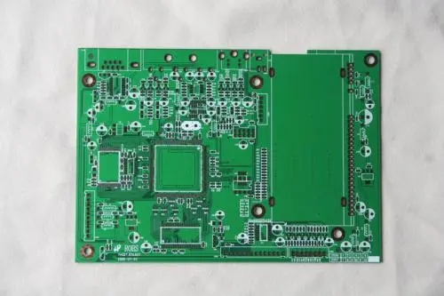
Normally, the number of PCB layers used for wearable devices ranges from 4 to 8. Layer is constructed by the principle that if it is an 8-layer PCB, it should provide enough strata and power layers and clamp the wiring layers in the middle. In this way, the ripple effect in crosstalk can be minimized and the electromagnetic interference (EMI) can be significantly reduced.
In the circuit board layout design phase, layout schemes generally place large strata close to the power distribution layer. This results in very low ripple effect and system noise can be reduced to almost zero. This is particularly important for RF subsystems.
FR4 has a higher dissipation factor (Df) than Rogers material, especially at high frequencies. For higher performance FR4 stacks, the Df value is about 0.002, which is an order of magnitude better than that of normal FR4 stacks. Rogers, however, have only 0.001 or smaller layers. When the FR4 material is used for high frequency applications, there is a significant difference in the insertion loss. Interpolation loss is defined as the loss of power from point A to point B when FR4, Rogers, or other materials are used.
PCB manufacturing problems
Wearable PCBs require stricter impedance control, which is an important factor for wearable devices, and impedance matching can produce cleaner signal transmission. Earlier, the standard tolerance for signal-carrying routes was (+) 10%. This indicator is obviously not good enough for today's high-frequency high-speed circuits. The requirement is now (+) 7%, in some cases even (+) 5% or less. This parameter, along with other variables, can severely affect the manufacture of wearable PCBs with very strict impedance control, thereby limiting the number of businesses that can make them.
The dielectric constant tolerance of the layers made of Rogers UHF materials is generally (+) 2%, some products can even reach (+) 1%, compared with 10% for FR4 layers. Therefore, comparing these two materials, it is found that the insertion loss of Rogers is especially low. The transmission loss and insertion loss of the Rogers stack are half as low as that of the conventional FR4 material.
Cost is most important in most cases. However, Rogers can provide relatively low-loss, high-frequency stacking performance at an acceptable price. For commercial applications, Rogers can be made into a mixed PCB with FR4 based on epoxy resins, some of which use Rogers and others use FR4.
Frequency is the primary consideration when selecting Rogers stacks. PCB designers tend to choose Rogers materials when the frequency exceeds 500 MHz, especially for RF/microwave circuits, because these materials can provide better performance when the above lines are subject to strict impedance control.
Compared with FR4 materials, Rogers materials also provide lower dielectric loss, and their dielectric constants are stable over a wide frequency range. In addition, the Rogers material can provide ideal low loss performance for high frequency operation.
The thermal expansion coefficient (CTE) of Rogers 4000 series materials has excellent dimensional stability. This means that when PCB undergoes a cold, hot and very hot reflux soldering cycle compared with FR4, the expansion and contraction of the printed circuit board can remain at a stable limit at higher frequencies and higher temperatures.
In the case of hybrid layers, it is easy to mix Rogers with high-performance FR4 using common manufacturing process technology, which makes it relatively easy to achieve high manufacturing yield. Rogers stacking does not require a dedicated hole preparation process.
Ordinary FR4 cannot achieve very reliable electrical performance, but high-performance FR4 materials do have good reliability, such as higher Tg, are still relatively inexpensive and can be used in a wide range of applications, from simple audio design to complex microwave applications.
PCBRF/microwave PCB design considerations
Portable technology and Bluetooth pave the way for RF/microwave applications in wearable devices. Today's frequency range is becoming more dynamic. A few years ago, very high frequency (VHF) was defined as 2GHz~3GHz. But now we can see UHF applications ranging from 10 GHz to 25 GHz.
Therefore, for wearable PCBs, the RF part requires more close attention to wiring issues, separating the signals separately so that the high frequency signals are generated away from the ground. Other considerations include providing a bypass filter, sufficient decoupling capacitance, grounding, and nearly equal design of transmission and loop lines.
Bypass filter can suppress the ripple effect of noise content and crosstalk. The decoupling capacitance needs to be placed closer to the pin of the device that carries the power signal.
High-speed transmission lines and signal loops require a layer between the power layer signals to smooth the jitter generated by noise signals. At higher signal speeds, small impedance mismatches can cause unbalanced transmission and reception of signals, resulting in distortion. Therefore, special attention must be paid to impedance matching related to radio frequency signals, because they have high speed and special tolerance.
RF transmission lines require impedance control to transfer RF signals from a specific IC substrate to a PCB. These transmission lines can be implemented on the outer, top and bottom layers, or they can be designed on the middle layers.
The methods used in the PCB RF design layout are microstrip lines, suspended striplines, coplanar waveguides, or grounding. A microstrip line consists of a fixed length of metal or line and a whole or part of a plane directly below it. The characteristic impedance in general microstrip line structures ranges from 50_to 75_.
Suspended strip lines are another method of wiring and noise suppression. The line consists of a fixed width wiring on the inner layer and a large ground surface above and below the central conductor. The ground level is clamped in the middle of the power layer, which provides a very effective grounding effect. This is a preferred method for wearable PCB RF signal wiring.
Coplanar waveguides provide better isolation near RF lines and lines that need to be traveled close to each other. The medium consists of a central conductor and ground planes on or below it. The best way to transmit radio frequency signals is to suspend a strip line or coplanar waveguide. These two methods can provide better isolation between the signal and the RF line.
The so-called "through-hole fence" is recommended on both sides of a coplanar waveguide. This method provides a row of grounding holes on each metal floor of the central conductor. The main route that runs in the middle has fences on each side, thus providing a shortcut to the lower stratum for the return current. This method can reduce the noise level related to the high ripple effect of the radio frequency signal. The dielectric constant of 4.5 remains the same as that of the semi-cured FR4 material, while the dielectric constant of the semi-cured sheet - from the microstrip line, strip line or offset strip line - is about 3.8 to 3.9.
In some devices that use the ground level, blind holes may be used to improve decoupling performance of power capacitance and to provide shunt paths from the device to the ground. The shunt path to the ground can shorten the length of the hole, which can achieve two purposes: you not only create the shunt or ground, but also reduce the transmission distance of devices with small patches, which is an important RF design factor.