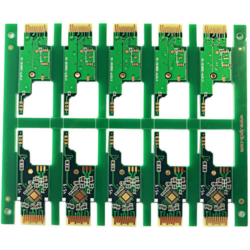
Through the above analysis of the parasitic characteristics of vias, we can see that in high-speed PCB design, seemingly simple vias often bring great negative effects to circuit design. In order to reduce the adverse effects caused by the parasitic effects of the vias, the following can be done in the design:

(1) Choose a reasonable via size. For multi-layer general-density PCB design, it is better to use 0.25mm/0.51mm/0.91mm (drilled holes/pads/POWER isolation area) vias; for some high-density PCBs, 0.20mm/0.46 can also be used For vias of mm/0.86mm, you can also try non-through vias; for power or ground vias, you can consider using a larger size to reduce impedance;
(2) The larger the POWER isolation area, the better, considering the via density on the PCB, generally D1=D2+0.41;
(3) The signal traces on the PCB should not be changed as much as possible, which means that vias should be reduced as much as possible;
(4) The use of a thinner PCB is beneficial to reduce the two parasitic parameters of the via;
(5) The power and ground pins should be made via holes nearby. The shorter the lead between the via hole and the pin, the better, because they will increase the inductance. At the same time, the power and ground leads should be as thick as possible to reduce impedance;
(6) Place some grounding vias near the vias of the signal layer to provide a short-distance loop for the signal.
Of course, specific issues need to be analyzed in detail when designing. Considering both cost and signal quality, in high-speed PCB design, designers always hope that the smaller the via hole is, the better, so that more wiring space can be left on the board. In addition, the smaller the via hole, its own The smaller the parasitic capacitance, the more suitable for high-speed circuits. In high-density PCB design, the use of non-through vias and the reduction in the size of vias have also brought about an increase in cost, and the size of vias cannot be reduced indefinitely. It is affected by PCB manufacturers' drilling and electroplating processes. Technical limitations should be given balanced consideration in the design of high-speed PCB vias.