Years of drawing experience of a PCB design engineer

1. PCB design layout/wiring, the impact on electrical performance is often seen in books about electronics, "digital ground wire and analog ground wire should be separated". Everyone who has deployed the board knows that this is a certain degree of difficulty in actual operation. To design a better board for the circuit board, you must first have an electrical understanding of the IC you are using, and which pins will generate higher harmonics (the rise/fall of digital signals or switching square wave signals). Edge), which pins are easy to induce electromagnetic interference, the signal block diagram (signal processing unit block diagram) inside the IC helps us understand.
The overall layout of the PCB design is the primary condition for determining the electrical performance, and the layout between the PCB boards is more concerned with the direction or flow of the signal/data between the ICs. The main principle is the part close to the power supply that is prone to electromagnetic radiation; weak signal processing Part of it is mostly determined by the overall structure of the equipment (that is, the overall planning of the early equipment). The circuit board is designed as close as possible to the input end of the signal or the detection head (probe), which can better improve the signal-to-noise ratio for subsequent signal processing and Data recognition provides purer signals/accurate data.
2. PCB design copper platinum processing
Circuit board design high-frequency signal traces should be thin, not wide, short rather than long, which also involves layout issues (signal coupling between devices), which can reduce induced electromagnetic interference.
The PCB design data signal appears on the circuit in the form of pulses, and its high-order harmonic content is a decisive factor to ensure the correctness of the signal; the same wide copper platinum will produce a skin effect on the high-speed data signal ( Distributed capacitance/inductance becomes larger), which will cause signal deterioration, incorrect data recognition, and inconsistent line widths in the data bus channel will affect data synchronization problems (leading to inconsistent delays), in order to better control the synchronization of data signals Problem, so a serpentine line appears in the data bus routing, which is to make the signal in the data channel more consistent in delay.
The large-area copper paving is aimed at shielding interference and inductive interference. The double-sided circuit board design can allow the ground to be used as the copper layer; while the multi-layer board does not have the problem of copper paving, because the power layer in between is very good Play a shielding and isolation role.
3. PCB design multi-layer board layout
Take the circuit board design for a four-layer board as an example. The power (positive/negative) layer should be placed in the middle, and the signal layer should be routed on the outer two layers. Note that there should be no signal layer between the positive and negative power layers. The advantage is to make the circuit board design power layer play the role of filtering/shielding/isolation as much as possible, and at the same time facilitate the production of the circuit board designer to improve the yield rate.
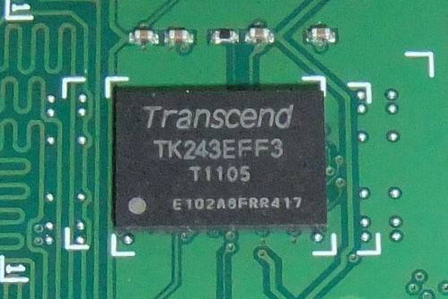
4. PCB design vias
PCB design should minimize the design of vias, because vias will generate capacitance, they are also prone to burrs.
Electromagnetic radiation. The aperture of the circuit board design via hole should be small rather than large (this is for electrical performance; but too small aperture will increase the difficulty of circuit board design and production, generally 0.5mm/0.8mm, 0.3mm should be used as small as possible), small The probability of burrs appearing after the copper immersion process is smaller for the hole diameter than that of the large hole diameter, which is caused by the drilling process.
5. PCB design software application
Each software for PCB design has its ease of use. Open a layer dedicated to expressing the openings, and then draw on this layer.
The desired opening shape should of course be filled with the drawn wire frame. This is to better allow circuit board designers and manufacturers
Identify your own statement and explain it in the sample documentation.
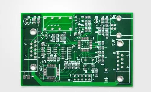
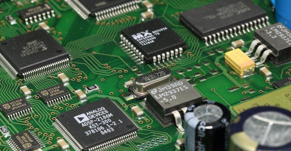
PCB design is widely known in electronic applications. As a qualified PCB design master, you should have comprehensive PCB design, PCB board wiring, PCB copy board and other comprehensive technologies. The following is a PCB studio Lao Xia, a 30-year PCB design senior engineer, summarized some technical information and guidelines on PCB design for the majority of PCB enthusiasts.
PCB design will have an impact on the following three effects:
1. The effect of electrostatic field before electrostatic discharge
2. Charge injection effect caused by discharge PCB copy board
3. Field effect produced by electrostatic discharge current
However, it mainly affects the third effect. The following discussion will give PCB design guidelines for the issues mentioned in Article 3.
Generally, the field coupling between receiving circuits can be reduced by one of the following methods:
1. Use a filter at the source to attenuate the signal copy board
2. Use a filter at the receiving end to attenuate the signal
3. Increase the PCB copy distance to reduce coupling
4. Reduce the antenna effect of the source and/or receiving circuit to reduce the PCB copy board coupling
5. Place the receiving antenna and the transmitting antenna vertically to reduce coupling
6. Add shielding between the receiving antenna and the transmitting antenna
7. Reduce the impedance of the transmitting and receiving antennas to reduce the electric field coupling
8. Increase the impedance of one of the transmitting or receiving antennas to reduce magnetic field coupling
9. Use a consistent, low-impedance reference plane (as provided by multi-layer PCB copy board) to couple signals to keep them in common mode
In specific PCB design, if electric field or magnetic field dominate, it can be solved by applying methods 7 and 8. However, electrostatic discharge generally generates an electric field and a magnetic field at the same time, which shows that Method 7 will improve the immunity of the electric field, but at the same time will reduce the immunity of the magnetic field. Method 8 is the opposite of the effect brought by method 7. Therefore, methods 7 and 8 are not perfect solutions. Regardless of whether it is an electric field or a magnetic field, using methods 1 to 6 and 9 will achieve certain results, but the solution of PCB design mainly depends on the combined use of methods 3 to 6 and 9.