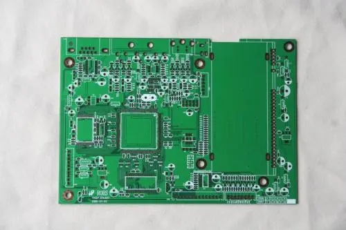
The wiring of the printed circuit board:
1. The layout of printed wires should be as short as possible, especially in high-frequency circuits; the bends of printed wires should be rounded, and right or sharp corners will affect high-frequency PCB circuits and high wiring density. Electrical performance; when wiring two panels, the wires on both sides should be perpendicular, oblique, or bent to avoid parallel to each other to reduce parasitic coupling; printed wires used as the input and output of the circuit should be avoided as far as possible. Parallel to avoid feedback, it is best to add a grounding wire between these wires.

2. The width of the printed wire: The width of the wire should meet the electrical performance requirements and be easy to produce. Its minimum value is determined by the current size, but the minimum should not be less than 0.2mm. In high-density, high-precision In the printed circuit, the wire width and spacing can generally be 0.3mm; the wire width should also consider its temperature rise in the case of large currents. The single-panel experiment shows that when the thickness of the copper foil is 50μm, the wire width is 1~1.5mm, and the current is 2A When the temperature rise is very small, the general selection of 1~1.5mm width wire may meet the design requirements without causing temperature rise; the common ground wire of the printed wire should be as thick as possible, and if possible, use a wire larger than 2~3mm Lines, this is particularly important in circuits with microprocessors, because when the ground wire is too thin, due to the change of the current flowing, the ground potential changes, and the level of the microprocessor timing signal is unstable, which will cause noise tolerance. Deterioration; 10-10 and 12-12 principles can be applied to the wiring between the IC pins of the DIP package, that is, when two wires pass between the two pins, the pad diameter can be set to 50mil, and the line width and line spacing are both 10mil When only one wire passes between the two pins, the pad diameter can be set to 64 mils, and the line width and line spacing are both 12 mils.
3. The spacing of printed conductors: the spacing between adjacent conductors must meet electrical safety requirements, and in order to facilitate operation and production, the spacing should also be as wide as possible. The minimum distance must be at least suitable for the withstand voltage. This voltage generally includes working voltage, additional fluctuating voltage, and peak voltage caused by other reasons. If the relevant technical conditions allow a certain degree of metal residue between the wires, the spacing will be reduced. Therefore, the designer should take this factor into consideration when considering the voltage. When the wiring density is low, the spacing of the signal lines can be appropriately increased, and the signal lines with high and low levels should be as short as possible and the spacing should be increased.
4. Shielding and grounding of printed wires: The common ground wire of printed wires should be arranged on the edge of the printed circuit board as much as possible. Keep as much copper foil as the ground wire on the printed circuit board. The shielding effect obtained in this way is better than that of a long ground wire. The transmission line characteristics and shielding effect will be improved, and the distributed capacitance will be reduced. . The common ground of the printed conductors is best to form a loop or a mesh. This is because when there are many integrated circuits on the same board, especially when there are more power-consuming components, the ground potential difference is generated due to the limitation of the pattern., Resulting in the reduction of noise tolerance, when it is made into a loop, the ground potential difference is reduced. In addition, the graphics of grounding and power supply should be as parallel as possible to the direction of data flow. This is the secret of enhancing the ability to suppress noise; multi-layer printed circuit boards can adopt several layers as shielding layers, and the power layer and ground layer are both visible. For the shielding layer, the ground layer and power layer are generally designed on the inner layer of the multilayer printed circuit board, and the signal wires are designed on the inner and outer layers.
The above is the introduction of PCB design experience. Ipcb also provides PCB manufacturers and PCB manufacturing technology.