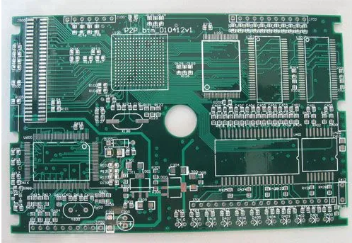
The layout principle of PCB design

The specification of PCB design directly affects the electrical performance of each process in the PCB manufacturing process and the board.
Excellent PCB design ability is a prerequisite for a qualified hardware engineer, and it is also an important indicator to measure the comprehensive quality of a hardware engineer.
In order to improve the standardization of PCB circuit board design and product yield, improve everyone's design ability, and speed up everyone's growth, the editor once again invited the big cow of Benqiang Circuit Design Division to talk with everyone about PCB design. Experience.
PCB layout principles of PCB design
Later, we will launch a series of articles on PCB design. Today, let’s talk about the layout design principles in PCB design and take a look at what requirements it has in this regard.
1) The distance from the edge of the board should be greater than 5mm.
2) Place the components that are closely related to the structure first, such as connectors, switches, power sockets, etc.
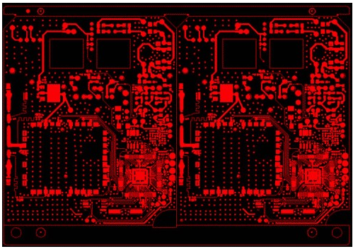
3) Prioritize the placement of core components and larger components related to circuit function modules, and then place the surrounding circuit electronic components with these core components as the center.
4) High-power electronic components should be placed on a circuit board that is conducive to heat dissipation. If a fan is used for heat dissipation, they should be placed on the mainstream air channel; if conductive heat dissipation is used, they should be placed near the chassis guide slot.
PCB layout principles of PCB design
5) High-quality components should not be placed in the center of the PCB board, preferably close to the fixed edge of the board in the chassis.
6) Components with high-frequency connection requirements should be put together as much as possible to reduce the distribution parameters of high-frequency signals and electromagnetic interference.
7) Keep input and output components as far away as possible.
8) The components with high voltage should be placed as hard as possible when debugging.
9) Thermal components should be far away from heating components to prevent these components from being heated and affecting their electrical performance.
10) The layout of adjustable components should be easy to adjust. Such as jumpers, variable capacitors, potentiometers, etc.
11) Consider the signal flow direction and arrange the layout reasonably to keep the signal flow direction as consistent as possible.
12) The layout of the PCB circuit board should be uniform, neat and compact.
PCB layout principles of PCB design
13) In the layout of surface mount components, pay attention to the same pad direction as possible to facilitate assembly and soldering and reduce the possibility of bridging.
14) The decoupling capacitor should be placed near the power input terminal.