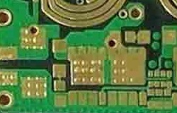
Heavy copper PCBs are made of 4 ounces or more of copper per layer. 4-ounce copper PCB is most commonly used in commercial products. The concentration of copper can reach up to 200 ounces per square foot. Heavy copper PCBs are widely used in electronic and electrical circuits that require high-power transmission. In addition, the thermal strength provided by these PCBs is impeccable. In many applications, especially in electronics, the thermal range is crucial because high temperatures can be destructive to sensitive electronic components and seriously affect circuit performance.

Heavy copper PCB is a type of circuit board with a copper thickness of ≥ 3oz/sq. On its outer and inner layers. The reason for classifying circuit boards as heavy copper PCBs is that their coating is thicker. In the production process of heavy copper PCB, the thickness of copper is increased by plating holes and sidewalls.
For example, when a PCB has 2 ounces of copper per square meter. Foot thick, it is a standard PCB. However, if it has more than 3 ounces of copper, it is a heavy copper PCB. Heavy copper PCB is considered a reliable wiring choice. Heavy copper PCBs are different from extreme copper PCBs in that they range from 20 ounces to 200 ounces per square meter.
How to manufacture heavy copper PCB?
For the manufacturing of heavy copper PCBs, electroplating or etching is usually used. The main purpose is to increase the copper thickness of the sidewalls and plating holes. The method used to manufacture heavy copper PCBs is not farfetched. Heavy copper PCB requires special etching and electroplating methods to ensure the additional thickness of copper.
Using ordinary etching techniques to manufacture heavy copper PCBs is not ideal. Ordinary etching methods can produce excessively etched edges and uneven edge lines. PCB manufacturers now use advanced etching and electroplating methods to achieve straight edges.
In the PCB manufacturing process, heavy copper PCBs are electroplated. This will help to thicken the PTH wall on the PCB. By using this technology, the number of layers is reduced and the impedance distribution is reduced. When the PCB is exposed to several cycles during the manufacturing process, the plating holes will weaken.
Method for manufacturing heavy copper PCB
1. Copper burial method
This method uses flat surfaces to manufacture thick copper PCBs. Here, heavy copper is inserted into the pre-impregnated resin. The thickness of the resin determines the thickness of copper.
For example, start with a 6mm laminate and a 10mm copper cladding. Then cover the copper coating with a photoresist. Afterward, use a 5 mil laser beam to cut the circuit pattern from the side of the laminate. The laser must be cut onto the copper foil through a laminate. If the laser is controllable, it can prevent damage to the copper foil.
Place the laminate into the electroplating bath for electroplating. After filling the laser cutting groove on the laminated board, the copper plating produces a copper plating thickness of approximately 6 mils.
2. Blue bar
Insert the thick copper bar into the circuit board. This method saves materials and reduces the weight of PCBs. During the manufacturing process, the resin flows into the space inside the copper wire, which helps to achieve a uniform top surface.
When it comes to multi-layer boards with heavy copper layers, attention must be paid to the copper filling level between the inner layers. Low levels of filling and resin can lead to resin starvation.
The difference between standard copper and heavy copper
Standard PCBs can be produced using copper etching and plating processes. These PCBs are plated to increase the copper thickness of planes, wiring, PTHs, and pads. The copper used for producing standard PCBs is 1oz. When producing heavy copper PCBs, the usage of copper is greater than 3oz.
For standard circuit boards, copper etching and electroplating techniques are used. However, heavy copper PCBs are produced through differential etching and step plating. Standard PCBs perform lighter activities, while heavy copper plates perform heavy tasks.
The conductive current of standard PCBs is lower, while that of heavy copper PCBs is higher. Due to its efficient heat distribution, thick copper PCBs are an ideal choice for high-end applications. Heavy copper PCBs have better mechanical strength than standard PCBs. Heavy copper circuit boards improve the performance of circuit boards that use them.
The Application of Heavy Copper PCB
Heavy copper PCBs are produced through etching and electroplating methods. The main purpose of producing this type of PCB board is to increase the thickness of copper through side walls and plate through holes. Heavy copper polychlorinated biphenyls have several benefits that contribute to their high demand.
Due to their outstanding characteristics and advantages, they can meet your electrical requirements. These circuit boards will always emit heat generated by high current conduction. Electronic products that use heavy copper plates have been in use for a long time. Heavy copper can carry large currents. These circuit boards will continue to meet the needs of various applications.
Heavy copper PCBs are widely used in various products because they provide multiple functions to improve circuit performance. These PCBs are widely used in high-power equipment such as transformers, heat sinks, inverters, military equipment, solar panels, automotive products, welding factories, and distribution systems.
Heavy copper PCBs generally require special pressing processes. It involves using multiple PP fillers during the pressing process to meet the required filling requirements. This pressing requires high pressure and a high flow of glue. There are blank areas in each layer of heavy copper PCB in the inner pattern; There is no copper in the open-air area. In addition, the edge of the board is designed with a single air duct.
Compared with ordinary PCBs, heavy copper PCBs have much higher heat dissipation capacity. Heat dissipation is crucial for developing robust and durable circuits.