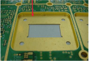
A cavity PCB refers to a hole (notch) that passes from the outer copper layer to the inner copper layer but does not fully penetrate the PCB. By assembling components in the cavity area, the height of the components can be reduced, making the entire circuit board more compact, and achieving more functionality and layout optimization in limited space. At the same time, the cavity can also provide more space, increase the gap between components, reduce interference between components, and improve the reliability and performance of the circuit.

Structure of cavity PCB
Compared to standard PCBs, cavity PCBs have structural grooves that allow for additional functionality. This feature allows for the insertion of heat sinks. These heat sinks are called "coins" and are used to locate electronic components below the surface. This makes the assembled printed circuit board as a whole thinner.
The surface of the inner cavity can also be used for electrical contact, usually a grounding connection. Although there are many methods for creating cavities in printed circuit boards, the most commonly used method is to mechanically remove materials from the PCB structure to create window-shaped cavities in multi-layer PCBs.
If the cavity is to be used as a microwave/RF resonant cavity, the frequency is determined by the size of the cavity, and the manufacturing of printed circuit boards must control the X, Y, and Z dimensions of the cavity. In addition, cavity design can be applied to many positions and different depths present on a PCB, and edge plating can also be performed.
Types of cavity PCBs
1) No copper plating or metallization inside the cavity
2) The top/bottom or walls (not both sides) of the chamber have copper. A cavity containing copper, such as traces and liners, is the most common type of cavity
3) The walls of the cavity were plated with copper, the floor was also plated with copper, and some of the walls were electroplated.
The advantages of cavity PCBs
*Reduce product size and weight
*Increase the density of product assembly
*Improve the overall performance of the product
*Meet the requirements of high-speed and highly informationized communication products
*Enhance the safety of surface components
*Increase heat dissipation area
Application Fields of Cavity PCB
*RF and Microwave Applications
*Telecommunications
*Central hybrid vehicle
*High current circuit
*Power amplifier
*DC power supply
*Motor control module
*Electric Vehicle Power System
*High-speed computing
In high-frequency antenna circuit boards, removing unnecessary circuit board layers can reduce the loss of high-frequency signals, which is particularly important for antenna structures. Therefore, PCBs with cavities are very suitable for wireless communication applications, such as smartphones and their infrastructure. By targeted material removal, waste heat generated by heating elements can also be more effectively managed.
As the size of printed circuit boards continues to shrink, the surface area available for wires and components becomes increasingly limited. In this case, a cavity PCB becomes an effective solution.