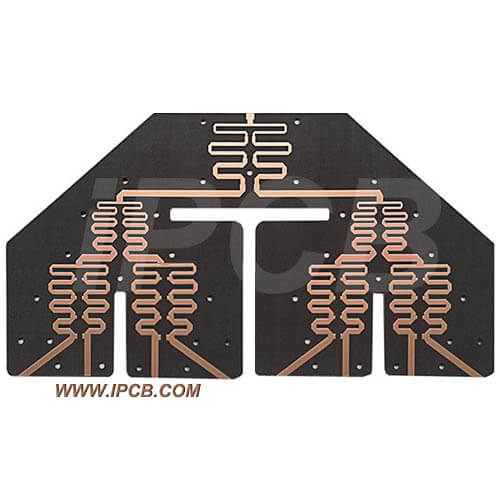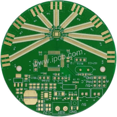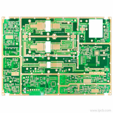


Product Name: Cavity PCB
Material: Teflon F4MB
Quality standard: IPC6012 Class 2
Dielectric constant: 2.55
Layers: 2Layers
Thickness: 1.5mm
Copper thickness: base copper 0.5oz, finished copper thickness 1oz
Surface technology: Immersion Silver
Application: Cavity PCB for power divider
Cavity PCB is used for power divider. A power divider is a device that divides the energy of one input signal into two or more channels to output equal or unequal energy. It can also combine the point of multiple signals into one work. It can also be called a combiner. A certain degree of isolation should be guaranteed between the output ports of a power divider. The main technical parameters of the power splitter include power loss (including insertion loss, distribution loss, and reflection loss), the voltage standing wave ratio of each port, the isolation between power distribution ports, power capacity and bandwidth, etc.
Cavity PCB microwave devices are characterized by small size, simple structure, and good applicability. At the same time, because the microwave device of the cavity PCB does not require any screw tightening, it can reduce costs, be easy to produce in batch, and avoid the potential of intermodulation products caused by fasteners such as screws.
Power splitters and combiners are the most common\most standard high-frequency devices, as are couplers such as directional couplers. These devices are used for power division, shunting, coupling high-frequency energy from the antenna or system interior with slight loss and leakage. The selection of Cavity PCB sheets is critical for these devices to achieve the desired performance. Therefore, when designing and processing power dividers/combiners/couplers, it is helpful to understand how the performance of the Cavity PCB material affects the ultimate version of these devices, such as helping to limit a range of different performance indicators for the selected sheet, including frequency range, working bandwidth, and power capacity.
When designing and processing high-frequency splitters/combiners and couplers, the selection of Cavity PCB materials should be based on several different fundamental material properties, including dielectric constant values, continuity of dielectric constant of materials, environmental factors such as temperature, and reducing material loss, including dielectric loss and conductor loss, as well as power capacity. Therefore, selecting Cavity PCB materials for specific applications will help successfully design high-frequency splitters/combiners or couplers.

Cavity PCB
A cavity coupler is used to distribute wired radio frequency signals on demand.
The primary purpose of a cavity coupler is to distribute a limited radio frequency signal on demand. Cavity coupler has coupling loss which can be designed according to actual needs. It has the characteristics of working frequency bandwidth, small band interpolation loss, high isolation, small standing wave ratio, and beautiful appearance. Cavity coupler is suitable for long-term and stable areas such as base station coupling, high power signal coupling, indoor distribution system, etc. It is selected according to the operator's requirements. A cavity coupler is a component that divides optical signals from one optical fiber into several optical fibers. It belongs to the field of passive optical components. It can be used in telecommunication networks, cable TV networks, user loop systems, and area network.
Because the cavity coupler has no isolation resistance, the filling medium is air, and the heat dissipation is fast. As a result, it can withstand relatively large power, the maximum capacity can reach 200W, and the insertion loss is slight.
The cavity coupler frequency is generally 800-2500MHz, and the coupling degree (dB) is 5, 6, 7, 8, 10, 15, 20, 25, 30. The cavity power divider has two, three, and four power dividers.
1. 400MHz-500MHz frequency band two and three power divider, used in conventional radio communication, railway communication, and 450MHz wireless local loop system.
2. 800MHz-2500MHz frequency band two, three, and four microstrip series power dividers are used in GSM/CDMA/PHS/WLAN indoor coverage projects.
3. 800MHz-2500MHz frequency range two, three, and four cavity series power dividers are used in GSM/CDMA/PHS/WLAN indoor coverage projects.
4. 1700MHz-2500MHz frequency range two, three, and four cavity series power dividers are used in PHS/WLAN indoor coverage projects.
5. Microstrip two and three power dividers used in small-volume equipment in the range of 800MHz-1200MHz/1600MHz-2000MHz.

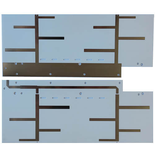
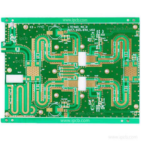
power divider contains cavity PCB
The power divider is widely used in wireless distribution systems. It can distribute the transmitted signal (Tx) of the base station into multiple antennas and send the password (Rx) received by the antenna back to the base station receiver simultaneously.
There are two standard two-way power dividers, Wilkinson PCB and cavity PCB.
Features of cavity PCB power divider and Wilkinson PCB power divider:
The cavity PCB power divider is generally a coaxial structure that transforms the input 50Ω impedance to 25Ω (using different inner and outer conductors). As a result, the 25Ω impedance can be well-matched with the parallel impedance of the two output 50Ω.
The Wilkinson PCB power divider is usually designed with a microstrip structure consisting of strip lines with a 1/4 wavelength impedance of 70.7Ω and a 100Ω resistor in series between the output ports.
Insertion loss is the natural enemy of wireless distribution system design. The inner conductor of the cavity power divider is made of brass, the surface is plated with silver, the shell is made of copper or aluminum, and the air medium is used. It can be considered the transmission line with the minor loss (except for superconducting). Usually, it is 0.05 dB or less, but it is generally marked as 0.1 dB because it is tough to test such a slight insertion loss. The microstrip power divider adopts a microstrip design and has an inherent loss of 0.3 to 0.5 dB. It doesn't sound significant, but the result is substantial after accumulating multiple power dividers.
For the reliability and safety of the cavity PCB system, for the microstrip power splitter, if the cable or antenna is damaged, it may cause an open circuit or short circuit of the splitter. But because of the isolation between the outputs, the problem of one arm will not affect the other arm. However, there is another situation where the Tx signal is reflected, and the Tx signal is many times larger than the Rx signal. Because the microstrip requires small size and its resistance rated power is also tiny, generally 100mw, there is no problem with consuming Rx signals, but when the circuit (antenna, cable) is open or short-circuited, the reflected Tx signal is enough to burn out This fragile resistance. Once the resistor is burned out, the power divider will not work typically, making it more difficult to recover the network. On the other hand, the cavity power divider has no burning resistance, so once the open circuit or short circuit problem is solved, the regular operation can be resumed immediately.
At the end of the PCB design process, it is decided whether to use the radio frequency interference shielding cavity, which often makes there is not enough space to join the shielding cavity, which causes the hole to affect other areas of the design in terms of physical structure.
For specific applications of cavity PCB, careful consideration of the above issues helps to choose the most appropriate and economical shielding form. Different four-sided shielded cavities can be selected for additional application requirements. The four-sided shielding cavity with a finger spring cover has fences on all four sides. By hand soldering, wave soldering, or through-hole reflow soldering, these fences and the series of pins on the edge of the PCB can weld the cavity to the PCB board. Finger spring covers are often used in this type of cavity. If the height of the fence is high enough to accommodate the finger spring, then the finger spring cover is the best choice among the removable covers. The size of finger springs, such as standard height or low profile, can be produced according to requirements. If there is not enough space outside the fence to place the external finger spring, the internal finger spring should be used. Moreover, the outer finger spring and the inner finger spring having the same form on the opposite side can be mixed and used.
Electronic equipment and radio frequency applications are ubiquitous in our daily lives. The regulations and directives of various regulatory agencies are changing day by day. It has never been more important to consider the radiation interference between independent components on the cavity PCB and adjacent circuits. The shielding of radiated interference should be regarded as other product design factors. It is best to view it early to avoid the expensive cost of PCB layout modification and equipment redesign to meet the initial electromagnetic compatibility test requirements. Other issues that need to be considered include product testing, shielding during production, further management instructions, such as RoHS regulations and costs.
In the cavity filter industry, to monitor data power, etc., or to shunt signals, many products will add cavity PCB coupling lines at the ant port for coupling to reach a specific coupling value, such as -35db, etc. When the coupling index requirements are substantial, the coupling line between the cavity PCB and the central pole is very long or very close. However, due to the limitation of the space structure, it is hoped that the cavity PCB will be small, so the coupling to be achieved is complex, especially for some filters with lower frequencies.
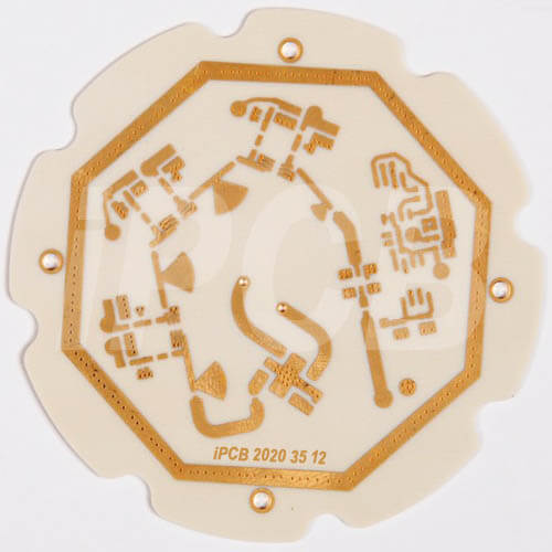
Product Name: Cavity PCB
Material: Teflon F4MB
Quality standard: IPC6012 Class 2
Dielectric constant: 2.55
Layers: 2Layers
Thickness: 1.5mm
Copper thickness: base copper 0.5oz, finished copper thickness 1oz
Surface technology: Immersion Silver
Application: Cavity PCB for power divider
For PCB technical problems, iPCB knowledgeable support team is here to help you with every step. You can also request PCB quotation here. Please contact E-mail sales@ipcb.com
We will respond very quickly.