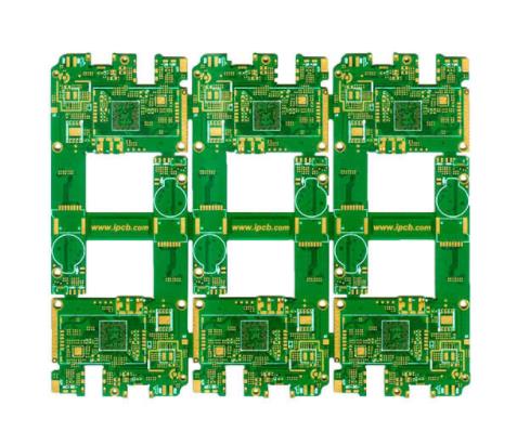
HDI stands for high-density interconnect, referring to circuit boards with higher wiring density per unit area than traditional circuit boards. Printed circuit board technology has been constantly evolving to meet the needs of smaller and faster products. HDI PCBs are more compact, with smaller through holes, solder pads, copper wires, and space. Therefore, HDI allows for denser routing, making PCBs lighter, more compact, and fewer layers. A single HDI board can accommodate the functionality of multiple boards previously used in the device. HDI PCB is the preferred choice for high-rise and expensive laminates.

The difference between HDI and regular PCB
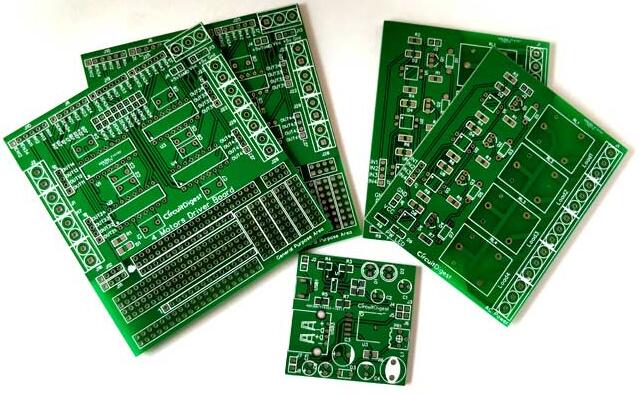
HDI (High-Density Interconnect Board) is a compact circuit board designed specifically for small-capacity users. Compared to regular PCBs, the most significant feature of HDI PCB is its high wiring density.
1. HDI PCB has a smaller volume and lighter weight
HDI board is made of traditional double-sided board as the core board, through continuous layering and lamination. This type of circuit board made by continuous layering is also known as a build-up Multilayer (BUM). Compared to traditional circuit boards, HDI PCB have advantages such as being light, thin, short, and small.
The electrical interconnection between HDI PCB boards is achieved through conductive through-hole, buried hole, and blind hole connections, which are structurally different from ordinary multi-layer circuit boards. Micro-buried blind holes are widely used in HDI boards. HDI uses laser direct drilling, while standard PCBs usually use mechanical drilling, so the number of layers and aspect ratio often decrease.
2. HDI motherboard production process flow
The high-density development of HDI PCB boards is mainly reflected in the density of holes, circuits, solder pads, and interlayer thickness.
1) Micro guide holes: HDI boards contain blind holes and other micro guide hole designs, which are mainly manifested in the high requirements of micro-hole forming technology with a pore size of less than 150um, as well as cost, production efficiency, and hole position accuracy control. In traditional multi-layer circuit boards, there are only through holes and no small buried blind holes.
2) Refinement of width and line spacing: mainly manifested in increasingly strict requirements for wire defects and wire surface roughness. The general line width and line spacing do not exceed 76.2um.
3) High pad density: The density of solder joints is greater than 50 per square centimeter.
4) Thinning of dielectric thickness: It mainly manifests in the trend of interlayer dielectric thickness developing towards 80um and below, and the requirement for thickness uniformity is becoming increasingly strict, especially for high-density boards and packaging substrates with characteristic impedance control.
3. HDI board has better electrical performance
HDI PCB can not only miniaturize terminal product design but also meet higher standards of electronic performance and efficiency simultaneously.
The increased interconnect density of HDI allows for enhanced signal strength and improved reliability. In addition, HDI PCB boards have better improvements in radio frequency interference, electromagnetic wave interference, electrostatic discharge, heat conduction, etc. HDI also adopts fully digital signal process control (DSP) technology and multiple patented technologies, which can adapt to loads in a full range and strong short-term overload capacity.
4. HDI boards have very high requirements for buried plug holes
The manufacturing threshold and process difficulty are much higher than ordinary PCBs, and there are also many issues to pay attention to during production, especially the buried hole plug hole.
HDI PCB is a high-end printed circuit board with very high line density and complexity, which can achieve high-speed signal transmission and reliable design. The main characteristics of HDI PCBs are multi-layer circuits, thin boards, small apertures, dense wiring, and micro-circuits, which are widely used in fields such as mobile phones, computers, network communication, and automotive electronics.