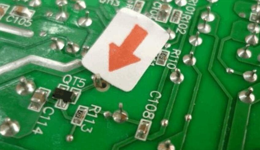
Reason 1. Copper foil shedding of PCB due to process factors of PCB manufacturer
PCB copper foil is overmatched. Currently, electrolytic copper foil used in PCB factories is generally single-sided galvanized (commonly called ashed foil) and single-sided copper plated. (commonly known as red foil), the common copper foil shedding is zinc-plated copper foil above 70um, red foil, and ashed foil below 18um, basically, there is no bulk shedding of copper foil. When the customer's PCB line is designed better than the etching line, if the copper foil specification changes and the etching parameters do not change, the copper foil will stay in the etching solution for too long. Zinc is originally a lively metal. When the copper wires on the PCB are immersed in the etching solution for a long time, it will cause the line to be over etched, which will cause the zinc layer on the back of some thin lines to be completely reacted off and separated from the base material, that is, the copper wires will fall off. Another case is that the PCB etching parameters are fine, but after etching, the copper wires are washed and dried poorly, resulting in the copper wires being surrounded by etching fluid residues on the PCB instant surfaces. If left untreated for a long time, the copper wires will be overmatched and the copper foil will fall off. This situation is generally manifested by concentrating on thin lines, or in wet weather, similar adverse effects will occur on the whole PCB. Strip off the copper wire to see that its color has changed with the base contact surface (so-called coarsening surface). Unlike the normal copper foil color, the original copper color at the bottom is seen, and the stripping strength of the copper foil at the thick line is also normal.
2. Local collision occurs during PCB production, and the copper wire is separated from the base material by external mechanical force. This is manifested by poor positioning or directionality, marked twisting of dropped copper wires, or scratches/impact marks in the same direction. If you look at the surface of the copper foil after peeling off the bad parts, you can see that the color of the copper foil surface is normal, there is no bad side etching and the peeling strength of the copper foil is normal.
3. Normally, as long as the high-temperature section of PCB is more than 30 minutes after hot pressing, the copper foil, and the semi-cured sheet will combine completely, so the bonding will not affect the binding force of the copper foil and the matrix in PCB. But they overlap on the laminate. During the stacking process, if PP is contaminated or copper foil surface is damaged, the bonding force between the copper foil and the base material after lamination will also be insufficient, resulting in positioning (for large plates only) or scattered copper wires falling off, but there will be no abnormal stripping strength of the copper foil near the stripping line.

Reason 2. Copper foil shedding from PCB due to customer's PCB design factors
1. The PCB line design is unreasonable. If the thick copper foil is used to design the thin line, the line will be overmatched and the copper foil will fall off.
Reason 3. Copper foil shedding of PCB due to PCB material
1. Common electrolytic copper foil is treated by zinc or copper plating on the foil. If the peak value of the foil is abnormal during production or when zinc/copper is plated, the coating crystal branch is bad, which results in insufficient peeling strength of the foil itself. When the bad foil-pressed sheet is made into PCB, the copper wire will fall off under external force impact when it is plugged in in the electronics plant. This type of copper foil does not peel off properly. It is shown that the wool face (i.e. the contact surface with the base material) of the copper foil does not show significant side corrosion, but the peeling strength of the whole copper foil is poor.
2. Copper foil has poor adaptability to resins: due to the different resin systems, the curing agent used for PCB with certain special properties, such as HTg sheet, is usually PN resin. The structure of the molecular chain of the resin is simple and the crosslinking degree is low when curing. It is necessary to use special peak copper foil to match it. The use of copper foil in the production of laminates does not match the resin system, resulting in insufficient peeling strength of the metal foil coated with PCB, and poor peeling of the copper wires in the plug-in.