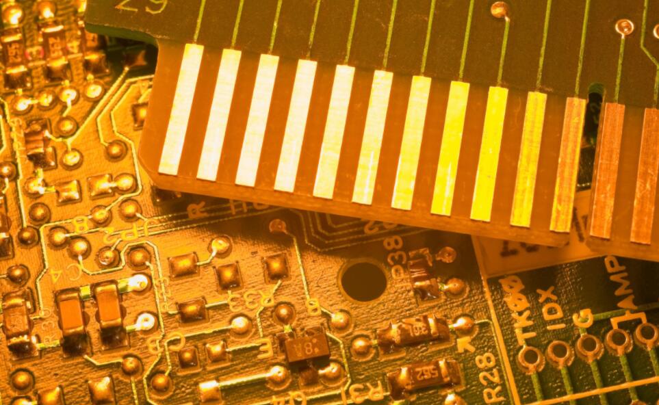
Electroplating is an essential process in the production of a PCB board. The coating of PCB boards varies according to the use of the boards. Here is a brief description of the properties and uses of copper and nickel coatings from the circuit board manufacturer IPCB.
1. Properties and uses of copper coating on PCB board
The copper coating of PCB is rosy, soft, ductile, easy to polish, and has good thermal conductivity and conductivity. However, it is easy to oxidize in the air and quickly loses its gloss, making it unsuitable as a "surface" layer for protective-decorative coatings.
The copper coating on the PCB board is mainly used as the "bottom" layer for multi-layer coating of steel and iron. It is also often used as the "bottom" layer for tin, gold and silver plating. Its function is to improve the binding force between the base metal and the surface or (or intermediate) coating, and also to facilitate the deposition of the surface coating. When the copper coating of PCB sheet has no holes, the corrosion resistance of the surface coating can be improved, for example, the advantages of using the plating process of thick copper and thin nickel in the protective-decorative multilayer plating can be explained here, and precious metal nickel can be saved.

2. Properties and applications of nickel coating on PCB board
Nickel metal has a strong passivation ability, can quickly generate a very thin passivation film on the surface of the parts, can resist atmospheric and some acid corrosion, so the nickel coating of PCB board has high stability in air. In the simple salt electrolyte of nickel, very fine crystalline coating can be obtained, which has excellent polishing performance. The polished PCB board nickel coating has a mirror-like gloss while maintaining its gloss in the atmosphere for a long time. In addition, the nickel coating of PCB board has higher hardness and wear resistance. According to the properties of nickel coating on PCB board, it is mainly used as the bottom layer, middle layer, and surface layers of protective-decorative coating, such as nickel-chromium coating, nickel-copper-nickel-chromium coating, copper-nickel-chromium coating, and copper-PCB board nickel coating.
Due to the high porosity of nickel coating on PCB board, only when the thickness of the coating is 25 μ When above m, there are no holes, so the nickel coating is not generally used as a protective coating.
The production of nickel coatings on PCB board is very large, and the consumption of nickel plating accounts for about 10% of the total nickel production worldwide.
3. Copper plating process for PCB circuit board
Eletcroless PlatingCoppe, also known as copper precipitation or porosification (PTH), is an autocatalytic oxidation-reduction reaction. First, the active particles on the surface of the insulating base are treated with an activator. The metal palladium particles are usually used (Palladium is a very expensive metal, which is expensive and has been increasing. In order to reduce the cost, a practical colloidal copper process is now in operation abroad). The copper ions are first reduced on these active metal palladium particles. These reduced copper nuclei themselves become catalytic layers of copper ions, enabling the reduction of copper to continue on the surface of these new copper nuclei. Electroless copper plating is widely used in our PCB manufacturing industry. At present, electroless copper plating is the most widely used method to metallize holes in PCB. The metallization process for PCB holes is as follows:
Drill hole+Abrasive board deburring+Top board ten holes cleaning treatment Ten pairs of wash+micro-etching chemical coarsening+Double wash-one preimmersion treatment One colloidal palladium activation treatment One pair of wash+gel removal treatment(acceleration)+Double wash+Copper immersion One pair of wash-down ten top board+Copper immersion 11 times Copper 10 wash once+Dry.