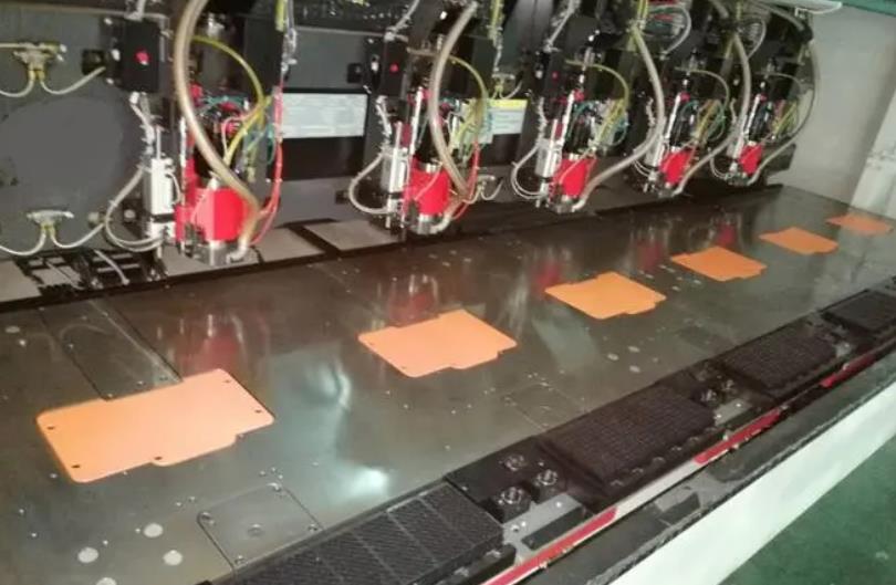
With the rapid development of the electronic industry market, various new products are emerging one after another, increasingly iterating and updating towards the direction of "light, thin, short, and small". PCB has also begun to develop towards high density, difficulty, and precision, as different types of through pcb drilling holes have emerged to meet the needs of the process. In the PCB production process, drilling is very important.
If the operation is improper, there may be problems with the through-hole process. The device cannot be fixed on the circuit board, which can affect its use. In severe cases, the entire board must be scrapped. The common drilling methods in printed circuit board PCBs nowadays include through holes, blind holes, and buried holes.

pcb drilling
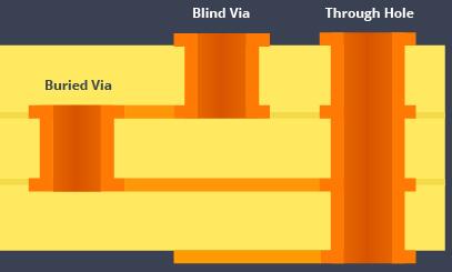
1. Through hole (VIA)
Copper foil lines used to conduct or connect conductive patterns between different layers of a circuit board, but cannot be inserted into copper plated holes of component leads or other reinforcing materials.
Tips: The conductive holes of the circuit board must pass through plug holes to meet customer needs. In changing the traditional aluminum sheet plug hole process, the circuit board surface resistance welding and plug holes are completed using white mesh, making their production more stable, quality more reliable, and application more perfect.
2. Buried hole
The connection between any circuit layer inside a printed circuit board (PCB), but without conduction to the outer layer, meaning that there are no conduction holes extending to the surface of the circuit board.
Tips: The production process cannot be achieved by bonding the circuit board and then drilling holes. It is necessary to drill holes at individual circuit layers, first partially bonding the inner layer, then electroplating treatment, and finally fully bonding. Usually only used for high-density circuit boards to increase the space utilization of other circuit layers.
3. Blind hole
Connect the outermost circuit and adjacent inner layers of a printed circuit board (PCB) with electroplated holes, as the opposite side cannot be seen.
Tips: Blind holes are located on the top and bottom surfaces of the circuit board, with a certain depth, used for connecting the surface circuit with the inner circuit below. The depth of the holes generally has a specified ratio (aperture). This production method requires special attention, and the drilling depth must be appropriate. Failure to pay attention can cause difficulties in electroplating inside the hole. Therefore, few factories adopt this production method.
4. Through Hole Design in High Speed PCB
Through the analysis of the parasitic characteristics of vias above, we can see that in high-speed PCB design, seemingly simple vias often bring significant negative effects to circuit design. In order to reduce the adverse effects of parasitic effects caused by vias, efforts can be made in the design to:
1) Considering both cost and signal quality, choose a reasonable size of the via hole. For example, for the 6-10 layer memory module PCB design, it is better to select 10/20Mil (drilling/pad) vias. For some high-density small size boards, you can also try to use 8/18Mil vias. Under current technical conditions, it is difficult to use smaller sized vias. For the via of the power supply or ground wire, larger sizes can be considered to reduce impedance.
2) The two formulas discussed above indicate that using a thinner PCB board is beneficial for reducing the two parasitic parameters of vias.
3) The signal wiring on the PCB board should not be changed layers as much as possible, which means that unnecessary vias should not be used as much as possible.
4) The pins of the power supply and ground should be perforated nearby, and the lead between the vias and pins should be as short as possible, as they can lead to an increase in inductance. At the same time, the power and ground leads should be as thick as possible to reduce impedance.
5) Place some grounded vias near the vias of the signal switching layer to provide a close circuit for the signal. It is even possible to place a large number of excess grounding vias on the PCB board.
Of course, flexibility is also needed in design. The through hole model discussed earlier refers to the situation where each layer has a solder pad, and sometimes we can reduce or even remove the solder pads of certain layers. Especially in cases where the density of vias is very high, it may lead to the formation of a groove in the copper layer that separates the circuit. To solve this problem, in addition to moving the position of the vias, we can also consider reducing the size of the solder pad of the pcb drilling in the copper layer.