Share three common types of PCB drilling. PCB drilling is a process and a very important step in PCB manufacturing. The main task is to drill holes for PCBs, such as through holes for wiring, structure, and positioning; Multi layer PCB drilling is not done all at once. Some holes are buried in the circuit board, while others are drilled through on the PCB, so there will be one drill and two drills.
What is the use of PCB drilling process?
PCB drilling is to connect the outer circuit with the inner circuit, and the outer circuit is connected to the outer circuit. Anyway, PCB drilling is to connect the circuits between different layers. In the later electroplating process, copper plating can be applied to the holes to connect the circuits between different layers. Some PCB drilling is for screw holes, positioning holes, row holes, etc., and their respective purposes are different.
PCB drilling is to drill the required through holes on the copper clad plate. Through holes mainly provide electrical connections and serve as fixing or positioning devices.
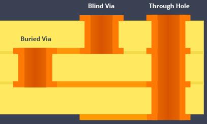
Let's first introduce the common PCB drilling methods in PCB: through hole, blind hole, and buried hole. The meanings and characteristics of these three types of holes.
Through hole (VIA) is a common type of hole used to conduct or connect copper foil circuits between conductive patterns in different layers of a circuit board. For example (such as blind holes, buried holes), but cannot be inserted into copper plated holes of component leads or other reinforcing materials. Because PCBs are formed by stacking and accumulating many layers of copper foil, an insulation layer is placed between each layer of copper foil, so that the copper foil layers cannot communicate with each other, and their signal connections rely on through holes (via).

PCB drilling
The characteristic is that in order to meet customer needs, the conductive holes of the circuit board must be plugged. This changes the traditional aluminum sheet plugging process by using white mesh to complete the resistance welding and plugging holes on the circuit board surface, making it stable in production, reliable in quality, and more comprehensive in application. Conducting holes mainly serve to connect and conduct circuits. With the rapid development of the electronics industry, higher requirements have been put forward for the production process and surface mounting technology of printed circuit boards. The process of plugging through holes has been applied, and the following requirements should be met:
1. Copper can be present in the through hole, while solder resistance can be plugged or not.
2. There must be tin and lead inside the conducting hole, with a certain thickness requirement (4um), and there must be no solder blocking ink entering the hole, causing hidden tin beads in the hole.
3. The conducting hole must have solder blocking ink plug holes, which are not transparent, and must not have tin rings, solder beads, or flatness requirements.
Blind hole: It refers to the connection of the outermost circuit in a PCB with adjacent inner layers through electroplated holes, which are called blind holes because the opposite side cannot be seen. In order to increase the utilization of space between layers in PCB circuits, blind holes have been applied. That is, a through hole on a surface of the printed circuit board.
Characteristics: Blind holes are located on the top and bottom surfaces of the circuit board, with a certain depth, used for connecting the surface circuit and the inner circuit below. The depth of the holes usually does not exceed a certain ratio (aperture). This production method requires special attention to the depth of PCB drilling (Z-axis) to be appropriate. If not paid attention, it will cause difficulties in electroplating inside the holes, so it is almost not used in factories. It is also possible to drill holes in individual circuit layers that need to be connected beforehand, and finally glue them together. However, it requires relatively precise positioning and alignment devices.
Buried hole refers to the connection between any circuit layer inside a PCB that is not conductive to the outer layer, and also refers to a conductive hole that does not extend to the surface of the circuit board.
Feature: In this process, PCB drilling after bonding cannot be achieved. PCB drilling must be performed at individual circuit layers, with partial bonding of the inner layer followed by electroplating treatment before complete bonding. This requires more effort than the original through and blind holes, so the price is also the most expensive. This process is usually only used for high-density circuit boards to increase the usable space of other circuit layers.
In PCB production process, PCB drilling is very important and should not be careless. Because PCB drilling is to drill the necessary through holes on the copper clad plate to provide electrical connections and fix the device. If the operation is improper, there may be problems with the through-hole process. The device cannot be fixed on the circuit board, which can affect its use. In severe cases, the entire PCB must be scrapped. Therefore, the PCB drilling process is quite important.