Water cleaning technology is the development direction of cleaning technology in the future, and it is necessary to set up pure water source and discharge water treatment workshop. It uses water as the cleaning medium, and adds surfactants, additives, corrosion inhibitors, chelating agents, etc. to the water to form a series of water-based cleaning agents. The PCBA water cleaner can be used to remove water solvents and non-polar contaminants.
PCBA cleaning machine technology
1. The characteristics of the cleaning process are:
(1) Good safety, non-flammable, non-explosive, and basically non-toxic;
(2) The formulation of the cleaning agent has a large degree of freedom, and it is easy to clean both polar and non-polar pollutants, and the cleaning range is wide;
(3) Multiple cleaning mechanisms. Water is a polar solvent with strong polarity. In addition to dissolution, it also has saponification, emulsification, displacement, and dispersion. The use of ultrasound is much more effective than in organic solvents;
(4) As a natural solvent, its price is relatively low and its sources are wide.

2. The disadvantages of water cleaning are:
(1) In areas where water resources are scarce, because this cleaning method consumes a lot of water resources, it is restricted by local natural conditions;
(2) Some components cannot be cleaned with water, and metal parts are easy to rust;
(3) The surface tension is large, it is difficult to clean small gaps, and it is difficult to completely remove the residual surfactant;
(4) It is difficult to dry and consumes a lot of energy;
(5) The cost of the equipment is high, a wastewater treatment device is required, and the equipment occupies a large area.
3. Semi-aqueous cleaning technology for PCB copy board
Semi-aqueous cleaning mainly uses organic solvents and deionized water, plus a certain amount of active agent, a cleaning agent composed of additives. This type of cleaning is between solvent cleaning and water cleaning. These cleaning agents are organic solvents, flammable solvents, relatively high flash point, relatively low toxicity, relatively safe to use, but must be rinsed with water, and then dried. Some cleaning agents add 5% to 20% of water and a small amount of surfactant, which not only reduces the flammability, but also makes rinsing easier. The characteristics of the semi-aqueous cleaning process are:
(1) The cleaning ability is relatively strong, which can remove polar and non-polar pollutants at the same time, and the cleaning ability is strong;
(2) Two different media are used for cleaning and rinsing, and pure water is generally used for rinsing;
(3) Dry after rinsing.
4. PCBA copy board scanning process
Since PCB copy board involves a problem of copy board accuracy, for circuit boards with high precision requirements such as mobile phone boards, it is necessary to copy out high-precision PCB layouts. In the scanning process, the scanner needs to be accurately selected and set. First, ensure the accuracy of the original scanned image. It can be said that the accuracy of the copy board mainly depends on the original scanning accuracy.
4.1 PCB scanning
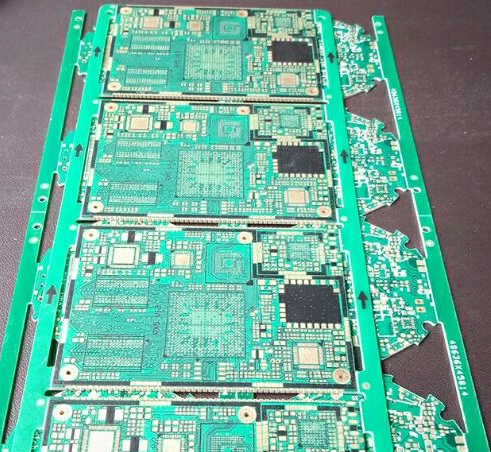
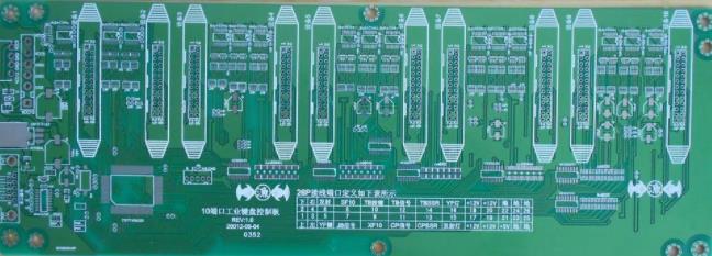
In the PCB copying process, PCB scanning is undoubtedly the first step of all processes. To get a good PCB board, it must be scanned by a computer first, and the relevant parameters and the original PCB layout must be backed up. After dismantling the board, get the split PCB light board, and formally enter the stage of copying the board. The first thing to do is to scan to store and record the PCB image. One thing to mention here is that in order to ensure that the relevant parameters on the PCB are clearly visible after scanning, the stains and residual tin on the surface of the PCB should be removed before scanning.
4.2 Significance of PCBDPI
Here, it is necessary to introduce a concept of DPI, the meaning of DPI is the number of dots per inch. That is to say, the distance between every two points on the scanned image is 1000/DPI, the unit is mil. Then, in the mobile phone board copying, the DPI is set to 1000 when the PCB is scanned, and the distance between two points on the image is 1000/1000=1mil, which means that the accuracy at this time is 1mil.
One thing to note is that the higher the accuracy of the scanned picture, the larger the picture and the higher the hardware requirements. Therefore, the DPI setting needs to be set according to the specific conditions of the original board to ensure that the next steps in the copying process can be Play the best results.
5. PCBA copy board related issues
How about a PCB copy board? What is a PCB copy board? A PCB copy board chip decryption? What tools are needed for a PCB copy board? How to copy a PCB circuit board? Getting started with a PCB copy board?