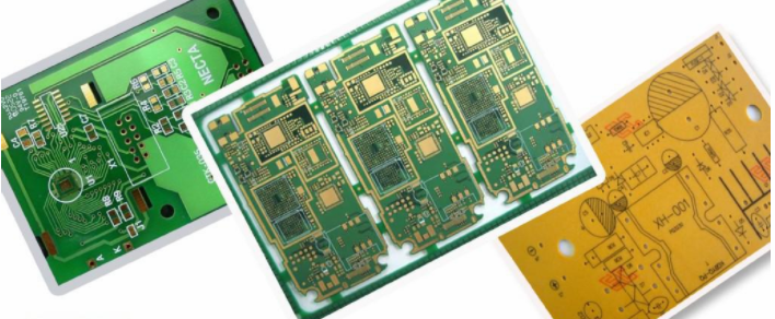
The realization process of PCB copy board technology is simply to scan the PCB circuit board to be copied, record the detailed component location, and then remove the components to make the bill of materials (BOM) and arrange the material purchase, and the empty PCB board is The scanned picture is processed by the copy board software and restored to a PCB board drawing file, and then the PCB file is sent to the plate making factory to make the board. After the board is made, the purchased components are soldered to the made PCB board, and then the circuit board is tested And debugging.
The specific steps of PCB copy board:
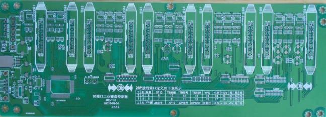
(1) The smt technical engineer got a PCB circuit board, and first recorded the model, parameters, and positions of all vital parts on the paper, especially the direction of the diode, the triode, and the direction of the IC gap; then use the digital camera Take two photos of the location of vital parts. Now the PCB circuit boards are getting more advanced. The diode transistors on the above are a little inadvertent, so they can't be seen at all and are easy to be ignored.

(2) Remove all the components and parts of the PCB copy board, and remove the tin in the PAD hole, and then clean the PCB circuit board with alcohol, and then put it into the scanner for scanning, and the scanner performs the process on the PCB circuit board. When scanning, you need to slightly increase the scanned pixels in order to get a clearer image, and then lightly sand the top and bottom layers with water gauze paper until the copper film is shiny, put it in the scanner, start PHOTOSHOP, and color the two Scan the layers separately; note that the PCB circuit board must be placed horizontally and vertically in the scanner, otherwise the scanned image cannot be used.
(3) Adjust the contrast and brightness of the canvas to make the part with copper film and the part without copper film have a strong contrast, then turn the second image into black and white, check whether the lines are clear, if not, repeat this step; if Clear, save the picture as black and white BMP format files TOP.BMP and BOT.BMP, if you find any problems with the graphics, you can use PHOTOSHOP to repair and correct them.
(4) Convert the two BMP format files to PROTEL format files respectively, and transfer to two layers in PROTEL. For example, the positions of PAD and VIA after the two layers basically overlap, indicating that the previous steps are well done. If there is Deviation, repeat the third step. Therefore, PCB copying is a work that requires patience, because a small problem will affect the quality and the matching degree of PCB copying.
(5) Convert the BMP of the TOP layer to TOP.PCB, pay attention to the conversion to the SILK layer, which is the yellow layer, and then you can trace the line on the TOP layer, and place the device according to the drawing in the second step. After drawing Delete the SILK layer and keep repeating until all the layers are drawn.
(6) Import TOP.PCB and BOT.PCB in PROTEL and combine them into one picture and it will be OK.
(7) Use a laser printer to print the TOP LAYER and BOTTOM LAYER on the transparent film (1:1 ratio), put the film on the PCB circuit board, and compare whether there is an error. If it is correct, it will be completed successfully. NS.
A copy of the PCB circuit board, which is the same as the original PCB circuit board, was born, but this is only half completed, and it needs to be tested to test whether the electronic technical performance of the PCB copy board is the same as that of the original board.