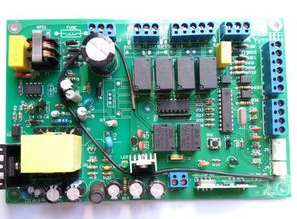
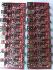
What are the characteristics of smt patch processing technology? Let's take a look at its characteristics with the smt chip processing factory.
1. Electronic products are small in size and high in assembly density
The volume of SMT chip components is only about 10% of traditional package components, and the weight is only 10% of traditional plug-in components. SMT technology can generally reduce the volume of electronic products by 40% to 60%, reduce the mass by 60% to 80%, and greatly reduce the area and weight. The grid of SMT patch processing and assembly components has developed from 1.27mm to the current 0.63mm grid, and some have reached 0.5mm grids. Adopting through-hole mounting technology can increase the assembly density.
2. High reliability and strong anti-vibration ability
SMT chip processing uses chip components, which have high reliability, small size, light weight, strong anti-vibration ability, automatic production, high installation reliability, and the rate of bad solder joints is generally less than 10 parts per million. The wave soldering technology of through-hole plug-in components is one order of magnitude lower, which can ensure the low defect rate of solder joints of electronic products or components. At present, nearly 90% of electronic products use SMT technology.

3. Good high frequency characteristics and reliable performance
Because the chip components are firmly mounted, the devices are usually leadless or short leads, which reduces the influence of parasitic inductance and parasitic capacitance, improves the high-frequency characteristics of the circuit, and reduces electromagnetic and radio frequency interference. The maximum frequency of the circuit designed with SMC and SMD can reach 3 GHz, while the chip component is only 500 MHz, which can shorten the transmission delay time. It can be used in circuits with a clock frequency above 16MHz. If the MCM technology is adopted, the high-end clock frequency of the computer workstation can reach 100 MHz, and the additional power consumption caused by the parasitic reactance can be reduced by 2-3 times.
4. Improve productivity and realize automated production
At present, in order to realize the complete automation of the perforated printed board, it is necessary to expand the area of the original printed board by 40%, so that the insertion head of the automatic plug-in can insert the component, otherwise there is not enough clearance, and the parts will be damaged. The SMT automatic placement machine (SM421/SM411) uses vacuum nozzles to suck and release components. The vacuum nozzle is smaller than the shape of the component, which increases the installation density. In fact, small components and fine-pitch QFP devices are produced by automatic placement machines to achieve full-line automatic production.
5. Reduce costs and reduce expenses
(1) PCB printed board use area is reduced, the area is 1/12 of through-hole technology, if CSP installation is used, its area will be greatly reduced; (2) Reduce the number of printed board holes and save rework costs ; (3) Due to the improvement of frequency characteristics, circuit debugging costs are reduced; (4) Due to the small size and light weight of chip components, packaging, transportation and storage costs are reduced; SMT chip processing technology can save materials, energy, and equipment, Manpower, time, etc., the cost can be reduced by up to 30% and 50%! !