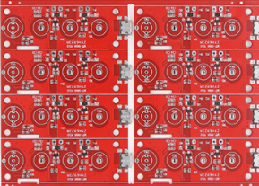
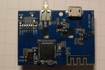
About PCBA factory automatic X-ray detector
X-rays have strong penetrability and are the earliest instruments used in various testing occasions. X-ray perspective images can show the density distribution of solder joint thickness, shape and mass. These indicators can fully reflect the welding quality of the solder joints, including open circuits, short circuits, holes, holes, internal bubbles and insufficient tin, and can be quantitatively analyzed. X-rays are generated by a micro-focus X-ray emission tube, pass through a window in the tube, and are projected onto the test sample. The X-ray absorption rate of the sample depends on the composition and proportion of the materials contained in the sample. The X-rays passing through the sample bombard the iodine coating on the X-ray sensitive panel and excite photons. These photons are detected by the camera to generate a signal, which is processed and amplified, and further analyzed and observed by the computer. Different sample materials have different opacity coefficients to X-rays, and the processed gray-scale image can show the difference in density and material thickness of the inspected object.
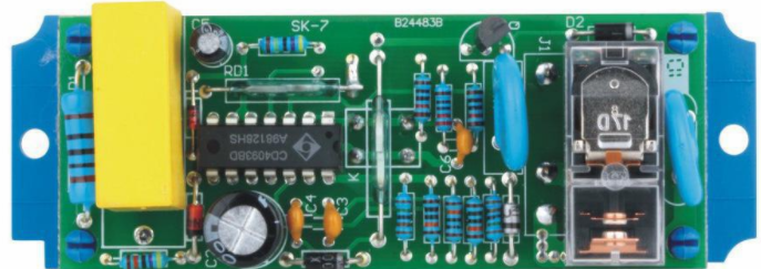
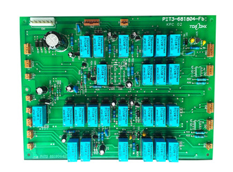
Definition and function of SMT process file
At present, there are two kinds of X-ray detectors that are used more frequently, one is a direct X-ray detector, and the other is a 3D-X-ray stratified scanning detector. The former is low in price, but can only provide two-dimensional image information, and it is difficult to analyze the masked part. The latter can detect the inherent defects of solder joints, hidden solder joint defects of BGA and other area array devices, and related inherent defects of the components themselves. 3D-X-ray layered scanning detector This detection technology uses scanning beam X-ray layered photography technology, which can obtain three-dimensional image information and eliminate shadows. It is combined with computer image processing technology to perform high-resolution detection of solder joints on the inner layer of PCB and SMA, and is especially suitable for detection of hidden solder joints under packaged devices such as BGA and CSP. Through the three-dimensional images of the solder joints, the three-dimensional size of the solder joints, the amount of solder and the wetting status of the solder can be measured, and the solder joint defects can be accurately and objectively determined. The quality of the metalized through holes of the printed circuit board can also be non-destructively tested . At present, the relatively advanced 3D-X-ray layered scanning detection technology still has certain limitations in practical applications, such as the detection of internal micro-cracks, which need to be further improved.

SMT patch AOI existing problems and future development trends
Although AOI has a higher efficiency than manual visual inspection, after all, the results are obtained through image acquisition and analysis and processing, and the related software technology of image analysis and processing has not yet reached the level of the human brain. Therefore, in actual use, some special situations, such as misjudgment and omission of AOI, are inevitable. Therefore, pattern recognition and intelligence will become the development direction of AOI technology.
1) Graphic recognition method has become the mainstream of application
As the main inspection objects (such as SMD components, PCB circuits, solder paste printing graphics, etc.) used in SMT for AOI technology are developing rapidly, it is difficult to fully keep up with the corresponding design rules and standards. For this reason, the DRC method based on design rules is difficult to apply, and the rapid development of computer technology has solved the problem of high-speed graphics processing, making the graphics recognition method more practical. At present, various AOI technologies of pattern recognition are more and more widely used in SMT.
2) AOI technology is developing towards intelligence
Under the characteristics of SMT's miniaturization, high density, rapid assembly, and diversified varieties, the amount of detection information is large and complex, whether it is in terms of real-time detection feedback, or in terms of the accuracy of analysis and diagnosis, it depends on manual labor. It is almost impossible to analyze and diagnose the quality information obtained by AOI, and intelligent AOI technology that replaces manual automatic analysis and diagnosis has become an inevitable development. The principle diagram of the intelligent AOI system adopts the solder joint shape recognition and expert system analysis. It is based on the solder joint morphology theory and method is similar to automatic visual inspection, that is, the optical system and image processing measures are used to measure the shape of the solder joint online. The computer compares the actual shape of the obtained solder joints with the reasonable shape of the system inventory, quickly identifies the faulty solder joints that exceed the allowable shape range, and uses intelligent technology to automatically analyze and evaluate their fault types and causes to form process parameter optimization adjustments Real-time control information, real-time feedback control of solder joint quality, and recording and statistics processing of analysis and evaluation information.