What is spray tin circuit board
PCB production editor: The so-called tin spraying is to soak the circuit board in molten tin and lead. When enough tin and lead is attached to the surface of the circuit board, hot air pressure is used to scrape off the excess tin and lead. After the tin-lead is cooled, the soldered area of the circuit board will be stained with a layer of tin-lead of appropriate thickness. This is the general procedure of the tin-spraying process. The surface treatment technology of PCB, currently the most widely used is the spray tin process, also called hot air leveling technology, which sprays a layer of tin on the pad to enhance the conduction performance and solderability of the PCB pad.
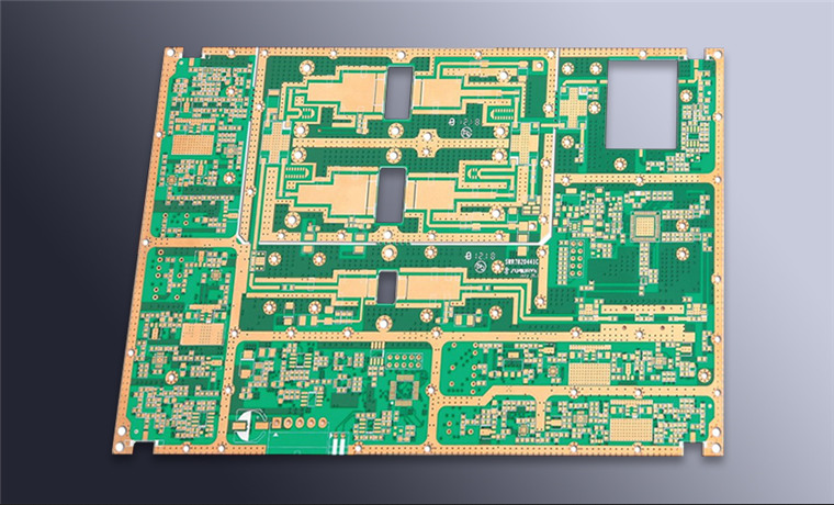
Tin spraying SMOBC&HAL) is the most common form of surface coating for circuit board surface treatment. It is widely used in circuit board production. The quality of spraying tin directly affects the quality of soldering and soldering during subsequent customer production. Solderability; therefore, the quality of tin spraying has become a key point of quality control for circuit board manufacturers. For general double-sided circuit boards, tin spraying and OSP anti-oxidation processes are the most used, while rosin technology is widely used on single-sided PCBs, and gold plating processes It is applied to the circuit board that needs to bond IC. Immersion gold is used more on the plug-in PCB board.

The main function of spray tin circuit board:
1. Prevent oxidation of the bare copper surface; copper is easily oxidized in the air, causing the PCB pad to be non-conducting or reducing the soldering performance. By applying tin on the copper surface, the copper surface can be effectively isolated from the air and maintain the conduction of the PCB. Versatility and solderability.
2. Maintain solderability; other surface treatment methods include: hot melt, organic protective film OSP, chemical tin, chemical silver, chemical nickel gold, electroplated nickel gold, etc.;
However, the cost-effectiveness of the tin-sprayed board is the best. The process characteristics of the tin-sprayed PCB board are that the tin-sprayed board includes two layers of copper and tin, which can adapt to poor environmental conditions and the soldering performance is better. It is more suitable in high temperature and corrosive environments. Seed boards are commonly used in industrial control equipment, communication products and military equipment products. The advantages of tin-spraying circuit boards: in the usual PCB surface treatment, the tin-spraying process is called the best solderability, because there is tin on the pad, When soldering tin, it is easier with gold-plated board or rosin and OSP process. This is very easy for us to solder by hand, and soldering is very easy.
The manufacture of tin-sprayed circuit boards:
In PCB manufacturing, for double-sided circuit boards and multi-layer circuit boards, if mass production, the most commonly used is to make tin-spraying process boards. If bonding or sinking gold PCB boards are not required, users are recommended to mass produce When using tin spraying process.