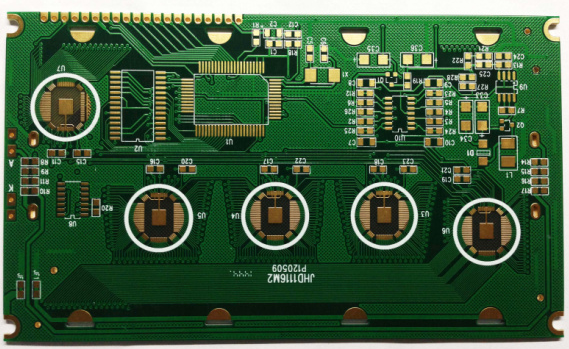
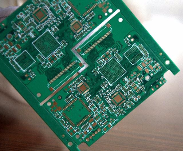
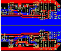
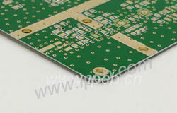
HDI circuit board, that is, high-density interconnection board, is a circuit board with high line distribution density that mainly uses micro-blind buried via technology. HDI circuit boards have inner and outer layers of circuits, and then use drilling, hole metallization and other processes to connect the inner layers of the circuits.
Generally speaking, HDI circuit board is specially designed for users with small capacity, because it is based on compact products and adopts modular and parallel design. In most cases, it adopts various patented technologies and digital signal processing technologies, and has strong short-term overload capacity and adaptable load capacity on a global scale.
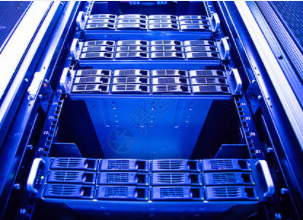
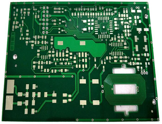
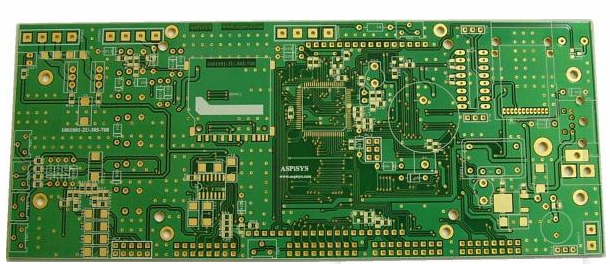
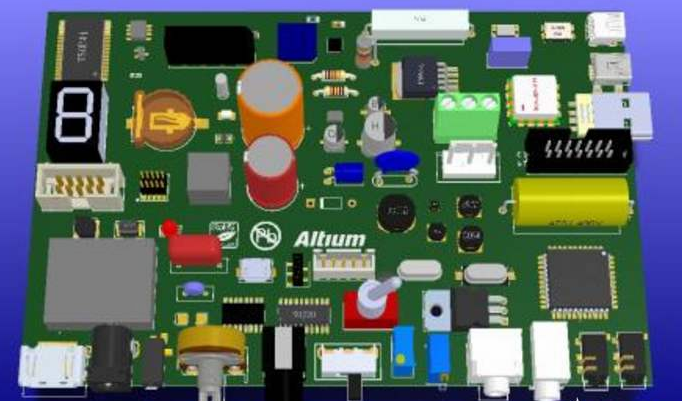
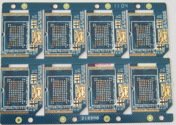
HDI circuit boards are generally manufactured by layer-by-layer method, the more the number of layers, the higher the technical grade of the board. Ordinary HDI circuit boards are basically laminated at one time, but high-end HDI circuit boards use 2 or more laminated technologies, while using advanced PCB technologies such as stacked vias, electroplating and filling, and laser direct drilling. High-end HDI circuit boards are mainly used in electronic equipment, such as mobile phones, advanced digital cameras, etc.
HDI circuit boards have many advantages. For example, in terms of improving product performance, HDI circuit boards can present lower noise from family planning appliances, minimize the structure of connection holes and circuit branches, and have stable voltage paths. Compared with other products It is closer to the distribution of capacitance, and can even play a role in blocking emission under certain circumstances.

In general, compared with ordinary PCBs, HDI circuit boards have better improvements in radio frequency interference, electromagnetic wave interference, electrostatic discharge, and heat conduction.
Nevertheless, HDI circuit boards still face new challenges, such as proofing technology. Due to the lack of relevant professionals in the market at present, it is impossible to estimate the stacking condition, price, and number of holes for HDI circuit boards at the beginning of the project design. At the same time, there is a certain jump in later assembly. Therefore, "reasonable selection of structure" has become a key factor between the performance and cost of HDI circuit boards.
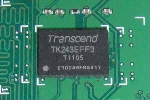
In the HDI circuit board proofing process, the selection of materials needs to be considered. In most cases, the raw materials for HDI PCB circuit board proofing are generally resins, and some of them will use modified acrylic resins, which are mainly determined by its main application place and environment.