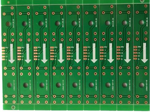
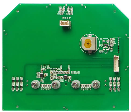
The increase in clock speed coupled with the high-frequency bus and higher interface data rate makes PC circuit board design more challenging. Engineers must go beyond the actual logic design on the board, and also consider other factors that may affect the circuit, including the size of the fingerprint module soft board circuit board, environmental noise, power consumption, and electromagnetic compatibility (EMC).
Hardware engineers should solve EMC problems in the PC circuit board design stage to ensure that the system will not be affected by EMC failures.
Good grounding design
Low-inductance grounding systems are the most important factor in minimizing EMC problems. Maximizing the grounding area on the PC circuit board can reduce the system grounding inductance, thereby reducing electromagnetic radiation and crosstalk.
Crosstalk can exist between any two wires on the circuit board, depending on the mutual inductance and mutual capacitance, and is proportional to the distance between the wires, the edge rate, and the wiring impedance.
In digital systems, the crosstalk generated by mutual inductance is usually greater than the crosstalk generated by mutual capacitance. Mutual inductance can be reduced by increasing the spacing between wiring or reducing the distance to the ground plane.
There are various ways to connect signals to ground. The circuit board design of the fingerprint module soft board factory where the components are randomly connected to the ground point will generate high ground inductance and cause inevitable EMC problems. We recommend using a fully paved ground plane, which can minimize the impedance when the current returns to the source, but the ground plane also requires a dedicated PC circuit board layer, which may be unrealistic for a double-layer circuit board.
Therefore, we recommend that designers use a ground grid . In this case, the inductance of the ground depends on the spacing between the grids.
In addition, the way the signal returns to the system ground is also important. If the signal path is long, it will produce a ground loop, which in turn will form an antenna and radiate energy. Therefore, all wiring that brings current back to the source should choose the shortest path and should go directly to the ground plane.
It is not advisable to connect all the different grounds and connect them to the ground plane. This will not only increase the size of the current loop, but also increase the possibility of ground bounce. Figure 1b presents the recommended method of connecting components to the ground plane.

Another good way to reduce EMC-related problems is to splice the ground with the complete edge of the circuit board to form a Faraday cage, so that no signal is routed outside the boundary . This method can limit the radiation of the circuit board of the fingerprint module soft board factory to the area within the limit, and avoid external radiation from interfering with the signal on the circuit board.
From an EMC perspective, the proper arrangement of the layers is also very important. If the number of layers used is more than two, use a complete layer as the ground layer. If a four-layer circuit board is used, the layer below the ground plane should be used as the power plane.
It must be noted that the location of the ground plane should be between the high-frequency signal wiring and the power plane. If a double-layer circuit board is used and a complete ground plane cannot be achieved, a ground grid can be used. If a separate power plane is not used, the ground wiring should be parallel to the power wiring to ensure clean power.
Layout guide
In order to protect the design from EMC, the components on the circuit board must be classified according to their functions (analog, digital, power supply, low-speed circuits, high-speed circuits, etc.). Each type of wiring should be in the designated area, and filters should be used at the boundary of the subsystem.
When dealing with digital circuit problems, special attention must be paid to clocks and other high-speed signals. The wiring that connects this signal should be as short as possible and should be adjacent to the ground plane to keep radiation and crosstalk under control.
For this kind of signal, engineers must avoid using vias or wiring at the edge of the circuit board or near the connector. In addition, the signal must also be far away from the power plane, as this will cause noise on the power plane. The wiring for transmitting differential signals should be as close as possible to each other, so that the magnetic field cancellation function can be exerted most effectively.
The wiring that transmits the clock signal from the source to the device should have matching terminals. As long as the impedance is not matched, signal reflection problems will occur. If you do not pay attention to the problem of reflected signals, a lot of energy will be radiated. Different forms of effective terminals include source point, end point, and AC terminal.
For the wiring facing the oscillator, other wirings other than ground should not run parallel to or below the oscillator or its wiring. In addition, the crystal should be close to the desired chip.
Since the return current always follows the path of the lowest reactance, the ground wiring that transmits the current should be close to the wiring that transmits the relevant signal, so as to keep the current loop as short as possible.
The wiring that transmits analog signals should be separated from high-speed or switching signals, and must be protected by grounding signals. A low-pass filter must always be used to remove high-frequency noise coupled to the surrounding analog wiring.
In addition, the ground planes of the analog and digital subsystems cannot be shared.

shield
Any noise on the power supply may affect the function of the device in operation. Generally speaking, the frequency of noise coupled to the power supply is high, so bypass capacitors or decoupling capacitors are required for filtering.
The decoupling capacitor provides a low impedance path for the high frequency current from the power plane to the ground. Current flows through a path to ground, and this path forms a ground loop. This path should be kept as low as possible, so the decoupling capacitor can be placed as close as possible to the IC.
Large ground loops increase radiation and may be a potential source of EMC failures. The higher the frequency, the closer the reactance of the ideal capacitor is to zero, and there is no so-called truly ideal capacitor on the market.
Lead and IC packaging also increase inductance. Multiple capacitors with low equivalent serial inductance can be used to improve the decoupling effect.
Many EMC-related problems are caused by cables that transmit digital signals. These cables actually function as highly efficient antennas. Ideally, the current entering the cable will flow out at the other end, but in fact parasitic capacitance and inductance will cause radiation problems.
The use of twisted-pair cables helps minimize coupling problems and eliminates any induced magnetic fields. If ribbon cables are used, multiple ground return paths must be provided. For high-frequency signals, shielded cables must be used, and the ground shield should be connected at the head and tail of the cable.
Shielding is a form of closed conductive container, which reduces EMI by weakening the E field and H field of the radiated wave. It can be connected to the ground, which can effectively reduce the size of the loop antenna by absorbing and reflecting part of the radiation. In this way, the shielding can also be used as a partition between the two zones, reducing the energy radiation from one zone to the other.
Finally, shielding is not an electrical solution, but a mechanical method to reduce EMC. Metal packaging (conductive and/or magnetic materials) can be used to avoid EMI from the system. We can use shielding to cover the entire system or part of the system, depending on the relevant requirements.