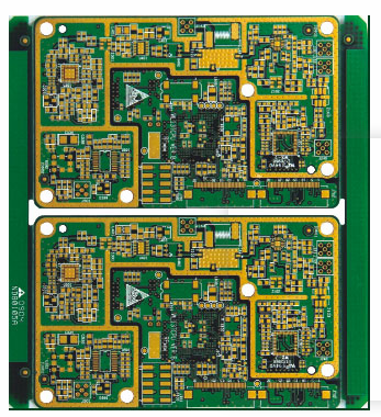
Many friends asked the editor, what are the most common surface treatment processes for PCB boards, and what are the advantages and disadvantages of each process. Here I will talk about it in detail.
The main surface treatment processes commonly used in PCB industry: Immersion gold, Immersion silver, Immersion tin, OSP, spray tin, gold plating, tin plating, silver plating. Different processes are selected according to different needs. The most important reference standard is cost, which is different. Process requirements and costs are different. According to your own cost requirements and functional requirements, you can choose a process that suits you. The most commonly used processes in several PCB processing are introduced below.

1, PCB surface spray tin treatment
The so-called tin spraying is to immerse the circuit board in molten tin and lead. When enough tin and lead is attached to the surface of the circuit board, hot air pressure is used to scrape off the excess tin and lead. After the tin-lead is cooled, the soldered area of the circuit board will be stained with a layer of tin-lead of appropriate thickness. This is the general procedure of the tin-spraying process. The surface treatment technology of PCB, currently the most widely used is the spray tin process, also called hot air leveling technology, which sprays a layer of tin on the pad to enhance the conduction performance and solderability of the PCB pad.
SMOBC&HAL), as one of the most common surface coating forms for circuit board surface treatment, is widely used in the production of circuits. The quality of tin spraying will directly affect the quality of soldering and soldering during subsequent customer production. Solderability; therefore, the quality of spray tin has become a key point of quality control for circuit board manufacturers. For general double-sided boards, the tin spraying and OSP processes are the most widely used, while the rosin process is widely used on single-sided PCBs, and the gold-plating process is used on circuit boards that require bonding ICs. Immersion gold is used more on plug-in boards.
In the usual PCB surface treatment, the tin spraying process is called the best solderability, because there is tin on the pad, when soldering the tin, it is easier to compare with the gold-plated board or the rosin and the OSP process. . This is very easy for us to solder by hand, and soldering is very easy.
2, PCB surface immersion gold treatment
The crystal structure formed by immersion gold is different from that of gold plating. Immersion gold will be golden yellower than gold plating, and customers will be more satisfied.
The crystal structure formed by immersion gold and gold plating is different. Immersion gold is easier to weld than gold plating, and will not cause poor welding and cause customer complaints.
Immersion gold board only has nickel and gold on the pads. In the skin effect, the signal transmission is on the copper layer and will not affect the signal.
Immersion gold has a denser crystal structure than gold plating, and it is not easy to produce oxidation.
Immersion gold board only has nickel and gold on the pad, so it will not produce gold wire and cause slight shortness.
Immersive gold board only has nickel and gold on the pads, so the solder mask on the circuit and the copper layer are more firmly bonded.
The project will not affect the spacing during compensation.
The crystal structure formed by immersion gold and gold plating is different, and the stress of the immersion gold plate is easier to control. For products with bonding, it is more conducive to bonding processing. At the same time, it is precisely because the immersion gold is softer than the gilding, so the immersion gold plate is not wear-resistant as the gold finger.
The flatness and stand-by life of the immersion gold board are as good as the gold-plated board.
3, PCB surface anti-oxidation (OSP) treatment
"OSP organic solderability preservatives" (OSP organic solderability preservatives) were called heat-resistant preflux in the early days. In essence, it is an alkyl benzimidazole (ABI alkyl benzimidazole) compound with high heat resistance, and its decomposition temperature is generally required to be above 300°C. Therefore, it can well protect the surface of fresh copper from oxidation and pollution. During high-temperature soldering, the OSP is removed due to the action of the solder to reveal the surface of the fresh copper and quickly weld firmly with the solder. But it is not suitable for multiple reflow soldering.
The basic principle of the "organic solderability protective agent is that the imidazole ring in the alkylbenzimidazole organic compound can form a coordination bond with the 2d10 electron of the copper atom, thereby forming an alkylbenzimidazole-copper complex. Among them, the chain alkyl groups are attracted to each other through Van der Waals force, so that a certain thickness (usually between 0.3∽0.5μm) of a protective layer is formed on the fresh copper surface, plus the presence of benzene rings, so this The layer of protective film has good heat resistance and high decomposition temperature.
The schematic diagram of the formation of "alkylbenzimidazole-copper complexes" is shown in Figure 4, where the choice or combination of R groups (alkyl) will determine whether it can be used as an OSP for PCBs. The choice of alkyl (R) will affect the heat resistance and decomposition temperature of OSP. Therefore, the chain length and structure of alkyl (R) are the main topics in the research and development of OSP, and it is also the continuous improvement of the heat resistance of OSP. And the main content of increasing the decomposition temperature is the main reason for the confidentiality of the OSP supplier.
4, PCB surface gold plating treatment
With the increasing integration of IC, the more IC pins become denser. The vertical spray tin process is difficult to flatten the thin pads, which brings difficulty to the placement of SMT; in addition, the shelf life of the spray tin plate is very short. The gold-plated board just solves these problems: for the surface mount process, especially for 0603 and 0402 ultra-small surface mounts, because the flatness of the pad is directly related to the quality of the solder paste printing process, and it plays a role in the quality of the subsequent reflow soldering. The decisive influence.
Therefore, the whole plate gold plating is common in the high-density and ultra-small surface mount process. In the trial production stage, due to factors such as component procurement, it is often not that the board is soldered immediately, but often it is often used for several weeks or even months. The shelf life of the gold-plated board is better than that of lead-tin alloy . Gold is many times longer, so everyone is willing to use it. Besides, the cost of gold-plated PCB in the sample stage is almost the same as that of lead-tin alloy board.
But as the wiring becomes denser and denser, the line width and spacing have reached 3-4MIL, which brings about the problem of gold wire short circuit; as the frequency of the signal becomes higher and higher, the signal is transmitted in the multi-plated layer due to the skin effect The more obvious the impact of the situation on the signal quality. (Skin effect refers to: high frequency alternating current, the current will tend to concentrate on the surface of the wire)