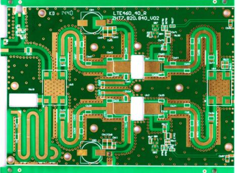
A notable trend is the ever-increasing bandwidth requirements ofhigh-frequency electronic products and modern data transmission circuits, as well as a strong push for integrated modules to reduce costs and improve performance. This means that traditional coaxial cable connectors cannot play an important role in high-frequency large-scale components. However, connection solutions for test applications and measurement applications require frequencies up to 110 GHz, and higher frequencies are required in the design phase. In order to solve these problems, a solderless printed circuit board mounting Rosenberger precision connector was developed.
The usual implementation type of surface mount connectors is right-angle mounting or edge mounting. These two types are suitable for all communication industries that require impedance control and good shielding performance. Their results are reliable, excellent, and repeatable. However, as it moves to a very high frequency, that is, the wavelength of the transmitted signal is comparable to the size of the connector, there is no need to consider the coupling resonant structure of the signal path.
This means that careful control of potential resonance and radiation at the connector and circuit board interface is critical to predicting performance. The wavelength is 3mm at 100GHz in vacuum, and the resonance of 1/4 wavelength (0.75mm) and half wavelength (1.5mm) must be controlled. The voids and gaps are small compared to these dimensions, and the wavelength in the printed circuit board medium is smaller.

Substrate thickness
In order to work in modeless, the thickness of the substrate must be much smaller than 1/4 wavelength. Given the substrate material, the ratio of the microstrip line width to the substrate thickness is constant. Therefore, the size of the millimeter wave circuit should not exceed a few tenths of a millimeter and is electrically connected by the center probe of the surface mount connector.
For example: Calculate the S parameters of the edge-mounted connector, as shown in Figure 1. Figure 1 shows that the signal performance is good before 25GHz. However, a strong resonance appeared at 30 GHz. This is caused by the parasitic resonant structure, which is coupled to the transmission line through the gap between the connector and the printed circuit board ground. This structure absorbs the main part of the signal, forming a deep narrow band that is reduced by about a few dBs in the insertion loss, and at the same time forming a spike in the reflection loss.
The main part of the signal radiates to free space, which may cause potential interference to adjacent circuits. The logarithmic field diagram of Figure 2 shows that the resonant fringe field passes through the ground gap. Emphasizes its physical model. Its performance is similar to a waveguide switch with signal probes, and its function is similar to that of an inductance column. Below we will consider how to deal with these challenges.
Technical characteristics
Figure 3 depicts the topology of the selected connector. The RF ground and the top layer ground are connected through many vias to keep the printed circuit board modeless. The area of the connector is on the top ground plane. This makes the connector package very simple and easy to design, and at the same time does not excite resonance during conversion.
For strip lines, the "pentip" type signal contact only generates a very low capacitive load, which is a necessary condition for the minimum reflection at high frequencies. The ground plane does not need a gap, otherwise it will make the design cumbersome. When the signal pins are led out from the mounting surface of the connector, once the connector is installed, elastic force will be applied to the signal pad, providing a stable and vibration-proof connection.
Features
• Connectors are: RPC-2.92 (40GHz) 02K80A-40ML5, RPC-1.85 (70GHz) 08K80A-40ML5 and RPC-1.00 (110GHz) 01K80A-40ML5
• No welding required
•Preset positioning pins
•The clamping device can accommodate a wide range of board thicknesses while providing a continuous ground connection between the contact surface and the circuit board
•Universal, reliable and reusable
As expected by the simulation, the test results confirmed the excellent RF performance of the new connector series up to 40GHz, 70GHz and 110GHz. The reflection loss and insertion loss of the three products are shown in Figures 4a and 4b, respectively. The frequency response has a modeless up to 110GHz. The insertion loss is 50% of the loss of the coplanar waveguide on the printed circuit board. The actual insertion loss of the connector is quite low. On the same substrate, the 70GHz and 110GHz versions have been tested. The 40GHz version is designed separately.
This explains the lower loss of 02K80A-40M at lower frequencies. This may only be due to different printed circuit board layouts. The TDR response of the 110GHz type connector is shown in Figure 5. The coaxial interface is on the left. This confirms good impedance control along the signal path. This type of connector has a wide range of applications in ultra-high frequency testing and measurement, and it also has a wide range of applications in the case of mandatory minimum radiation and coupling to adjacent circuits.