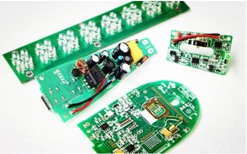
Inspection purpose: to verify the reliability of the solder joint strength of the products produced by PCBA.
Inspection method and process:
1. Visual inspection of solder joints
(1) Use tools: X-Ray, 3-D microscope
(2) Main inspection, X-Ray mainly inspects Solder Balls solder joint shape, short circuit, displacement, Void size, etc. of BGA, LGA, QFN and other parts; 3-D microscope mainly inspects the appearance of solder joints of lead leakage parts, and the angle of soldering. Etc., as well as the appearance of tin balls on the periphery of BGA parts, tin cracks, stolen goods, etc.
(3) Inspection frequency: X-Ray: For BGA and LGA products, 1pannel is inspected every 1K. 3-D microscope has been introduced: For BGA and LGA first pieces, the appearance of 5 particles on the four sides and the center is inspected. Used when analyzing defective products
(4) Inspection standard: Acceptance standard of Void size
IPC610D specification:
1. The bubble volume ≤ 25% of the tin ball volume is the acceptable bubble acceptance standard:
2. The bubble volume ≥ 25% of the tin ball volume is unacceptable
Solder Balls displacement judgment standard:
1: Solder ball offset PAD≤25% is an acceptable level
2: Solder ball offset PAD≥25% is unacceptable
Solder Balls Short Circuit Judgment Criteria: All short circuits are unacceptable even with tin
2. Solder joint strength inspection
(1) Tools used: push-pull machine and fixture
(2) Main inspection: resistance/capacitance/inductance/SOP, QFP and other original push-pull force measurement. Inspection frequency: inspection when new product/new original/new solder paste is introduced; when bad analysis
(3) Inspection standards: There are currently no inspection standards and empirical values in the industry, except for the requirements of customers alone.

3. Dye test
(1) Tools used: dye, vacuum pump, oven, 3-D microscope
(2) Main inspection: Whether the tin balls of BGA parts are intact and whether there is tin cracking
(3) Inspection frequency: inspection at the time of new product/new original/new solder paste introduction; at the time of failure analysis
(4) Inspection standards:
Crack (color display) is not allowed on PCBA that has not done any Reliability experiment.
PCBA Crack after Reliability experiment appears on the solder joint end layer ≤ 25% is acceptable.
4. Section Inspection
(1) Use tools: grinding machine, sealing material, sandpaper, polishing powder
(2) Main inspection: Cross-section observe the metallographic structure of the solder joints, as well as the IMC forming and the crystallization of the solder joints.
(3) Inspection frequency: inspection at the time of new product/new original/new solder paste introduction; at the time of failure analysis
(4) Inspection standards:
Slice Solder Ball, QFP, SOP sample inspection:
1: Solder ball offset PAD≤25% is an acceptable level
2: Solder ball offset PAD≥25% is unacceptable
3: Both short-circuit and empty welding at the solder joint ends are rejected.
4: Crack not allowed
5. Microstructure and element analysis
(1) Use tools: SEM electron microscope & EDX
(2) Main inspection: microstructure of solder joints, IMC thickness measurement, and surface element structure analysis
(3) Inspection frequency: inspection at the time of new product/new original/new solder paste introduction, and at the time of failure analysis
(4) Inspection standard: Solder Joint IMC thickness inspection:
PCBA PAD end: 2-5um, Component Substrate 1-3um
EDX judgment: usually Solder Ball and element composition are: Sn/Ag/Cu 96.5%/3.0/0.5 where the atomic ratio of C and O is normal at 10%. The content of element P of the IMC layer is about 9-11%, which is normal.