1. PCB design starts from determining the size of the board. Because the size of the printed circuit board is limited by the size of the chassis shell, it is appropriate to fit it into the shell. Secondly, consider the printed circuit board and external components. (Mainly potentiometers, sockets or other printed circuit boards) connection methods. The printed circuit board and external components are generally connected by plastic wires or metal isolation wires. But sometimes it is also designed as a socket. That is: to install a plug-in printed circuit board in the device, leave a contact position as a socket. For larger components mounted on printed circuit boards, metal accessories should be added to fix them to improve vibration and impact resistance.
2. The basic method of wiring diagram design first needs to have a complete understanding of the specifications, dimensions, area, etc. of the selected components and various sockets; reasonable and careful consideration of the location of each component, mainly from electromagnetic field compatibility The angle of performance, anti-interference, short wiring, less crossover, power supply, ground path and decoupling are considered. After the position of each component is determined, it is the connection of each component. Connect the relevant pins according to the circuit diagram. There are many ways to complete it. The design of printed circuit diagrams has two methods: computer-aided design and manual design.
The most primitive is to arrange the layout by hand. This is more laborious, and it often takes several iterations to complete it. This is also possible when there is no other drawing equipment. This manual arrangement of layout methods is also very helpful for those who are just learning the printing plate layout. Computer-aided drawing, now there are many kinds of drawing software with different functions, but generally speaking, drawing and modification are more convenient, and they can be saved and printed.

Next, determine the required PCB size, and according to the schematic diagram, initially determine the position of each component, and then continuously adjust the layout to make the layout more reasonable. The wiring arrangement between the components in the printed circuit board is as follows:
(1) Cross circuits are not allowed in printed circuits. For lines that may cross, you can use "drilling" and "winding" two methods to solve them. That is, let a lead "drill" through the gap under other resistors, capacitors, and triode pins, or "wind" from one end of a lead that may cross. In special circumstances, how complex the circuit is, it is also necessary to simplify the design. It is allowed to connect with wires to solve the problem of cross circuit.
(2) Components such as resistors, diodes, and tubular capacitors can be installed in "vertical" and "horizontal" installation methods. The vertical type refers to the installation and welding of the component body perpendicular to the circuit board, which has the advantage of saving space, and the horizontal type refers to the installation and welding of the component body in parallel and close to the circuit board, and its advantage is that the mechanical strength of the component installation is better. For these two different mounting components, the component hole pitch on the printed circuit board is different.
(3) The grounding point of the same level of circuit should be as close as possible, and the power filter capacitor of this level of circuit should also be connected to the grounding point of this level. In particular, the grounding points of the base and emitter of the transistor of this level should not be too far apart, otherwise the copper foil between the two grounding points will be too long, which will cause interference and self-excitation. Using such a "one-point grounding method" circuit will work better. Stable and not easily self-excited.
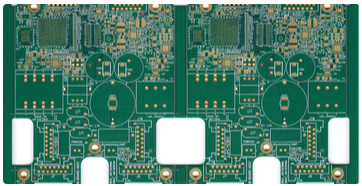
Printed circuit boards are structural elements formed by insulating materials supplemented by conductor wiring. When the final product is made, integrated circuits, transistors, diodes, passive components (such as resistors, capacitors, connectors, etc.) and various other electronic parts will be installed on it. Through the wire connection, the electronic signal connection can be formed and the application function can be formed. Therefore, the printed circuit board is a platform that provides component connection and is used to undertake the basis of connecting parts.
Since the printed circuit board is not a general terminal product, the definition of the name is slightly confusing. For example, the motherboard for personal computers is called the motherboard and cannot be directly called the circuit board. Although there are circuit boards in the motherboard, it is not They are not the same, so when evaluating the industry, the two are related but cannot be said to be the same. Another example: because there are integrated circuit parts mounted on the circuit board, the news media call it an IC board, but in fact it is not the same as a printed circuit board.
Under the precondition that electronic products tend to be multi-functional and complex, the contact distance of integrated circuit components has been reduced, and the speed of signal transmission has been relatively increased. This is followed by an increase in the number of wiring and the length of wiring between points. The performance is shortened, these require the application of high-density circuit configuration and microvia technology to achieve the goal. Wiring and jumper are basically difficult to achieve for single and double panels. Therefore, the circuit board will be multi-layered, and due to the continuous increase of signal lines, more power and ground layers are necessary means for design. All of these have made the Multilayer Printed Circuit Board (Multilayer Printed Circuit Board) more common.
For the electrical requirements of high-speed signals, the circuit board must provide impedance control with alternating current characteristics, high-frequency transmission capabilities, and reduce unnecessary radiation (EMI). With the structure of Stripline and Microstrip, multi-layer design becomes a necessary design. In order to reduce the quality problems of signal transmission, insulating materials with low dielectric coefficient and low attenuation rate are used. To cope with the miniaturization and arraying of electronic components, the density of circuit boards is continuously increased to meet demand. The emergence of component assembly methods such as BGA (Ball Grid Array), CSP (Chip Scale Package), DCA (Direct Chip Attachment), etc., has promoted printed circuit boards to an unprecedented high-density state.
Any hole with a diameter of less than 150um is called a microvia in the industry. The circuit made by the geometric structure technology of this microvia can improve the efficiency of assembly, space utilization, etc., and it is also useful for the miniaturization of electronic products. Its necessity.
For circuit board products of this kind of structure, there have been many different names in the industry to call such circuit boards. For example, European and American companies used to use sequential construction methods for their programs, so they called this type of product SBU (Sequence Build Up Process), which is generally translated as "Sequence Build Up Process." As for the Japanese industry, because the pore structure produced by this type of product is much smaller than the previous hole, the production technology of this type of product is called MVP (Micro Via Process), which is generally translated as "Micro Via Process." Some people call this type of circuit board BUM (Build Up Multilayer Board) because the traditional multi-layer board is called MLB (Multilayer Board), which is generally translated as "build-up multilayer board".
In order to avoid confusion, the IPC Circuit Board Association of the United States proposed to call this type of product the generic name of HDI (High Density Intrerconnection Technology). If it is directly translated, it will become a high-density connection technology. However, this cannot reflect the characteristics of the circuit board, so most circuit board manufacturers call this type of product HDI board or the full Chinese name "High Density Interconnection Technology". But because of the problem of the smoothness of spoken language, some people directly call this type of product "high-density circuit board" or HDI board.