PCB copy board according to the actual circuit board to push out the schematic diagram, BOM list and PCB file, and then carry out the PCB printing to make the PCB circuit board, and then purchase the components and carry out the PCBA processing. There are many introductions to copy board and PCBA processing, but it is not an easy task to do a good job in the later production of PCB copy board.
The two major difficulties in how to make a board after PCB copying are the processing of high-frequency signals and weak signals. In this regard, the level of PCB manufacturing is particularly important. The same principle design, the same components, and PCBs made by different people are very important. With different results, how can one copy out a PCB completely so that subsequent PCB proofing and batch processing can proceed normally?
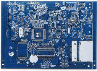
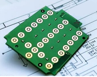
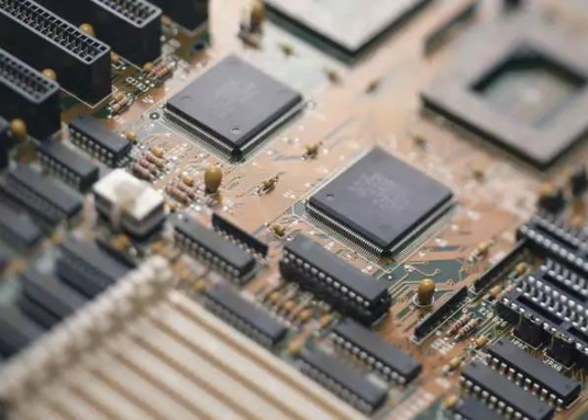
High-speed PCB copy board
1. Determine the PCB type of the copied board
The circuit board can be divided into ordinary PCB board, high frequency PCB board, small signal processing PCB board, and PCB board with both high frequency and small signal processing.

If it is an ordinary PCB board, as long as the layout and wiring are reasonable and tidy, and the mechanical size is accurate, if there are medium load lines and long lines, certain means should be used to deal with them to reduce the load. The long line should be strengthened and the focus is to prevent Long line reflections.
When there are signal lines exceeding 40MHz on the board, special considerations should be made to these signal lines, such as crosstalk between lines.
High-frequency PCB board copying has stricter restrictions on the length of wiring. According to the network theory of distributed parameters, the interaction between high-speed circuits and their wiring is a decisive factor, which cannot be ignored in system design. As the gate transmission speed increases, the opposition on the signal lines will increase accordingly, and the crosstalk between adjacent signal lines will increase proportionally. Generally, the power consumption and heat dissipation of high-speed circuits are also very large, so high-speed PCBs are being made. Enough attention should be paid when copying the board.
PCB copy boards with weak signals of millivolt or even microvolt levels require special attention to these signal lines. Small signals are too weak and are very susceptible to interference from other strong signals. Shielding measures are often necessary, otherwise they will Greatly reduce the signal-to-noise ratio. As a result, the useful signal is submerged by noise and cannot be extracted effectively.
The commissioning of the board should also be considered during the copying stage. The physical location of the test point, the isolation of the test point and other factors cannot be ignored, because some small signals and high-frequency signals cannot be directly added to the probe for measurement.
In addition, the number of layers of the PCB copy board, the packaging of components, the mechanical strength of the board, and subsequent PCB proofing also need to make corresponding references to the original circuit board.
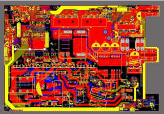
PCB copy board component layout
2. Requirement of component function on layout
Special components have special requirements in the layout and wiring, such as the analog signal amplifier used by LOTI and APH. The analog signal amplifier requires a stable power supply and small ripple. Keep the analog small signal part as far away from the power device as possible. On the OTI board, the small signal amplifying part is also specially equipped with a shielding cover to shield the stray electromagnetic interference. The GLINK chip used on the NTOI board uses ECL technology, which consumes a lot of power and generates heat. Special consideration must be given to the heat dissipation problem in the layout. If natural heat dissipation is used, the GLINK chip must be placed in a place with relatively smooth air circulation., And the heat radiated can not have a big impact on other chips. If the board is equipped with speakers or other high-power devices, it may cause serious pollution to the power supply. This point should also be paid enough attention.
3. Consideration of component layout
The layout of the components considers the electrical performance. The components with close connections should be put together as much as possible, the high-speed line layout should be as short as possible, and the power signal and small signal components should be separated.
On the premise of meeting the circuit performance, the components must be placed neatly and beautifully, which is convenient for testing. The mechanical size of the board, the location of the socket, etc. also need to be carefully considered.
The grounding in the high-speed PCB copy board and the transmission delay time on the interconnection line are also the first factors to be considered in the system design. The transmission time of the signal line has a great influence on the overall system speed, especially for high-speed ECL circuit board copying. Although the integrated circuit block itself is very fast, because the ordinary interconnection line (every 30cm line The delay amount of about 2ns) brings about an increase in the delay time, which can greatly reduce the system speed. Like shift registers, synchronous counters and other synchronous working components are best placed on the same plug-in board, because the transmission delay time of the clock signal to different plug-in boards is not equal, which may cause the shift register to produce a major error. On one board, where synchronization is the key, the length of the clock lines connected from the common clock source to the plug-in boards must be equal.
4. Wiring considerations
The transmission delay time of the transmission line is much shorter than the signal rise time, and the main reflections produced during the signal rise period will be submerged. Overshoot, recoil and ringing are no longer present. The MOS circuit board is copied from the board because the ratio of rise time to line transmission delay time is much larger, so the trace can be as long as meters without signal distortion. Logic circuits, especially ultra-high-speed ECL integrated circuits, due to the increase in edge speed, if no other measures are taken, the length of the trace must be greatly shortened to maintain signal integrity.
TTL adopts Schottky diode clamping method for the fast falling edge, so that the overshoot is clamped at a level that is one diode drop lower than the ground potential, which reduces the subsequent kickback amplitude, and the slower rising edge allows Overshoot, but it is attenuated by the relatively high output impedance (50-80Ω) of the circuit in the level "H" state. PCB copy board needs to consider the application and improvement of TTL. Due to the greater immunity of the level "H" state, the kickback problem is not very prominent. For HCT series devices, if Schottky diode clamping and series connection are used Combining the resistance termination method, the improvement effect will be more obvious.