PCB design should also streamline manufacturing. In the design process, the direction of the through-hole component, the landing type and the hole need to be considered. From assembly time, you can help your PCB manufacturer by placing fiducial marks on the circuit board. This helps speed up the assembly of the circuit board and reduce manufacturing/assembly errors.
Component orientation
When you think about it, certain components can be connected to the PCB in multiple ways. For simple components like resistors, orientation is not important; the device is not sensitive to signal polarity. Other components, such as square and rectangular ICs, can be placed on a circuit board with multiple orientations, and only one of these arrangements is correct.
Provide manufacturers/assemblers with some information about your right direction. Components and circuit boards are essential to ensure that the finished circuit boards are manufactured correctly and function as designed. The automatic pick and place machine needs some reference points to identify the correct position and orientation of the space plate. These reference points appear on the PCB in the form of fiducial marks.

The random copper strips on the PCB are actually an important feature to improve the profitability of the manufacturing process. The fiducial mark plays a dual role, providing a reference point for the placement machine and direction indicators for nearby components. There is no interchangeable direction for square and rectangular ICs, and your assembler can determine the correct direction based on the position of the nearby fiducial mark.
The square IC has a usable mark on one corner of the chip to indicate the correct orientation of the component on the board. Similarly, rectangular ICs have notches on one end of the chip to indicate their orientation. The fiducial mark can be placed on a corner or end of the area where the IC is to be mounted on the PCB. When properly oriented, the orientation notch on the IC will be adjacent to the fiducial mark.
Datum points and tool holes in grouping
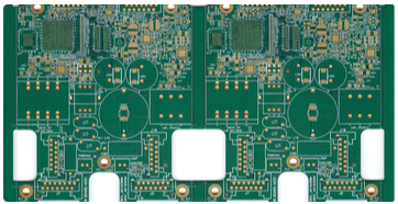
In addition to component placement, a fiducial mark can be placed on the panelized PCB to indicate the correct orientation of the panel. If you are manufacturing a rectangular board, you should place the fiducial marks at the opposite corners of the board and at the opposite corners of the panel. This allows pick-and-place machines or other assembly machines to determine whether the panels are loaded in the correct orientation.
The IPC standard requires you to place three reference points on the panel, one for each corner. This allows the pick and place machine to distinguish the entire panel from the individual panels. This also allows the pick and place machine to recognize whether the panel has been rotated by mistake.
The reference point can also be used to check the length of the PCB during the manufacturing process. The size of the PCB will be slightly different, and these changes will accumulate in the larger circuit board. A vision system can be used to measure the diagonal or lateral distance between two reference points and check the allowable tolerances. This allows pick-and-place machines or other assembly machines to reject boards that do not meet allowable tolerances.
If you are using a circuit board with surface mount components on both sides. On the circuit board, you need to place reference points on both sides of the circuit board. This allows the assembly machinery to locate appropriate references on both sides of the board. The same applies to paneled panels. The size of the fiducial mark you should place on the board depends on the capabilities of the assembly machinery. Again, please consult your manufacturer to understand their requirements.
If your PCB needs to be mounted on its packaging or other surface, you can choose to include various tool holes. Since the tool hole goes through the entire PCB, there should be enough clearance between the hole, nearby traces and any power/ground planes on the inner layer. Tool holes should remain unplated so that they are isolated from electrical connections and reduce the possibility of short circuits.
Place the connector
The connectors installed on the PCB by the PCB factory usually have an obvious direction. Connectors for external cables or devices usually appear on one edge of the circuit board and will point outward from the edge. When the outward-facing connector appears in the corner of the board, it can have two different directions. The fiducial mark can be used to indicate the correct orientation of the connector.
Vertical connectors, whether surface mount or through-hole connectors, also have specific directions that should be indicated directly on the board. These connectors are usually keyed, which forces the cable to be inserted in a specific direction. The fiducial mark can be used to indicate the position of the key relative to the connector hole or landing pad.